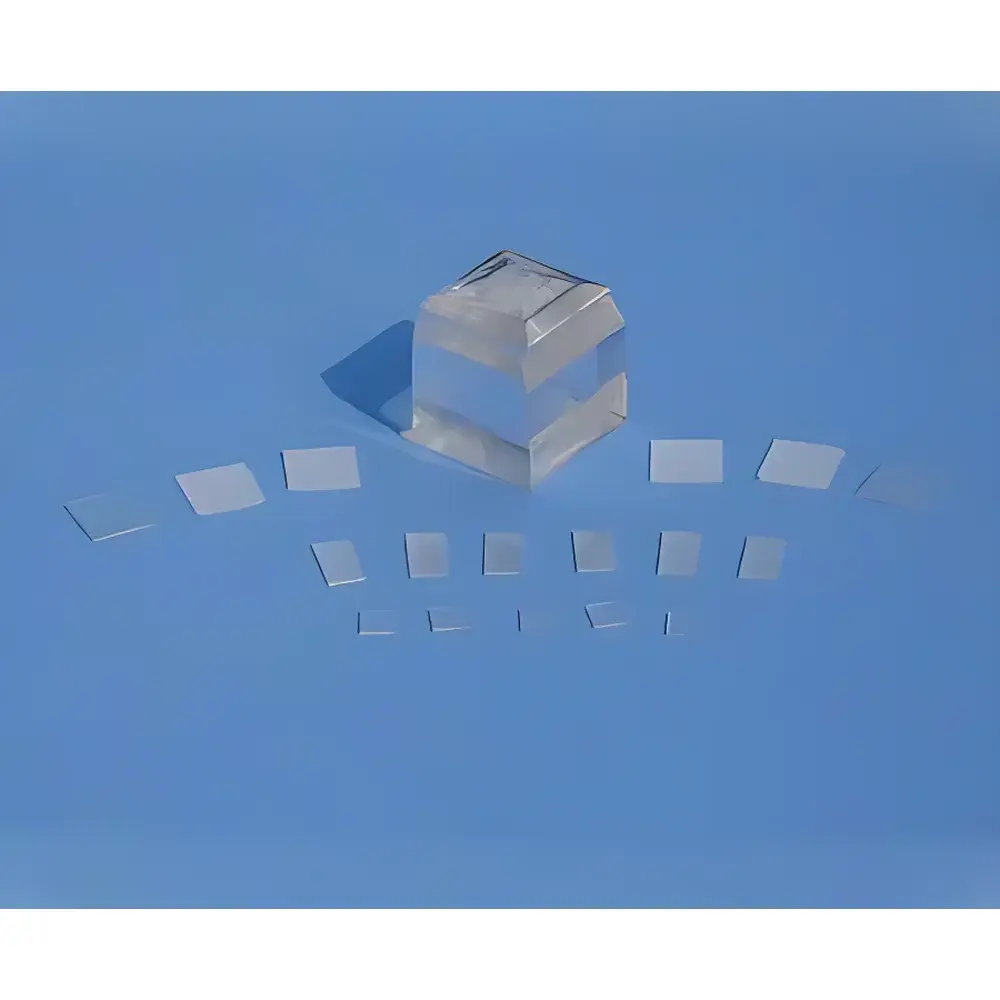
KTaO3 Potassium Tantalate Single Crystal Substrate
| Brand | Hefei Kejing |
|---|---|
| Origin | Anhui, China |
| Manufacturer Type | Authorized Distributor |
| Origin Category | Domestic (China) |
| Model | KTaO3 |
| Pricing | Upon Request |
| Molecular Weight | 268.04 g/mol |
| Crystal Structure | Cubic perovskite |
| Lattice Constant | a = 3.989 Å |
| Growth Method | Top-Seeded Melt Growth (TSMG) |
| Melting Point | ~1500 °C |
| Density | 7.015 g/cm³ |
| Mohs Hardness | 6 |
| Thermal Conductivity | 0.17 W/(m·K) @ 300 K |
| Refractive Index | 2.14 (at 589 nm) |
| Standard Orientations | <100>, <110>, <111> |
| Orientation Tolerance | ±0.5° |
| Standard Dimensions | 10 × 10 × 0.5 mm³, 10 × 5 × 0.5 mm³ |
| Surface Finish | Single- or double-side polished |
| Surface Roughness (Ra) | < 0.5 nm |
| Packaging | Class 1000 cleanroom processed, sealed in Class 100 clean bags |
Overview
The KTaO3 Potassium Tantalate Single Crystal Substrate is a high-purity, structurally stable perovskite oxide material engineered for advanced thin-film epitaxy, surface science investigations, and electrochemical sensing platforms. As a dielectric substrate with a centrosymmetric cubic lattice (space group Pm3̄m) and negligible intrinsic polarization, KTaO3 serves as an ideal template for the growth of functional oxide heterostructures—including high-temperature superconductors, multiferroics, and complex transition-metal oxides—where interfacial strain, symmetry matching, and lattice coherence are critical. Its wide bandgap (~3.5 eV), low dielectric loss, and thermal stability up to 1400 °C in inert atmospheres enable reliable operation in ultra-high vacuum (UHV) deposition systems (e.g., PLD, MBE, sputtering) and high-temperature electrochemical cell configurations. Unlike ferroelectric analogues such as BaTiO3 or LiNbO3, KTaO3 exhibits no spontaneous polarization below its quantum paraelectric regime (~10 K), making it uniquely suited for controlled interface engineering without built-in depolarization fields.
Key Features
- High structural fidelity: Single-crystal wafers grown via top-seeded melt growth (TSMG), ensuring low dislocation density (<104 cm−2) and uniform lattice parameter (a = 3.989 Å)
- Precise crystallographic orientation: Available in standard orientations , , and , with angular tolerance ≤ ±0.5°, verified by high-resolution X-ray diffraction (HR-XRD) rocking curve analysis
- Ultra-smooth surfaces: Chemomechanically polished to Ra < 0.5 nm (measured by atomic force microscopy), minimizing nucleation defects during thin-film deposition
- Thermally robust architecture: Maintains dimensional stability under rapid thermal cycling (up to 1000 °C/min) and sustained annealing at 1200 °C in O2/Ar environments
- Controlled stoichiometry: Verified by energy-dispersive X-ray spectroscopy (EDS) and Rutherford backscattering spectrometry (RBS), with K:Ta:O ratio deviation < ±1.2% from ideal 1:1:3
- Contamination-controlled handling: Processed and packaged in ISO Class 6 (1000) cleanroom; final sealing in ISO Class 5 (100) laminar-flow bags with residual particle count < 10 particles/ft³ (≥0.5 µm)
Sample Compatibility & Compliance
KTaO3 substrates are compatible with industry-standard wafer-handling protocols across semiconductor-grade toolsets, including load-lock chambers, robotic end-effectors, and cassette-based transport systems. All batches undergo full traceability documentation per ISO 9001:2015 quality management requirements. Substrates meet ASTM F1529–21 specifications for crystalline orientation verification and surface finish metrology. For regulated applications in pharmaceutical process analytical technology (PAT) or electrochemical biosensor development, substrates support GLP-compliant documentation packages, including CoA (Certificate of Analysis), CoC (Certificate of Conformance), and batch-specific HR-XRD spectra. No RoHS-restricted substances are introduced during polishing or packaging; lead-free, halogen-free processing confirmed per IEC 63000:2018.
Software & Data Management
While KTaO3 substrates are passive components, their integration into automated thin-film synthesis workflows benefits from interoperable data tracking. Each substrate lot is assigned a unique QR-coded identifier linked to a secure cloud-hosted database containing full metrological records: orientation maps (via Laue diffraction), surface topography scans (AFM), and optical transmission spectra (200–2500 nm). This dataset structure aligns with ISA-88/ISA-95 frameworks for materials traceability in GMP environments and supports audit-ready export in CSV, XML, or PDF/A-2 formats compliant with FDA 21 CFR Part 11 electronic record requirements.
Applications
- Epitaxial growth of correlated electron systems (e.g., La2CuO4, SrRuO3, BiFeO3) requiring lattice-matched, non-polar templates
- Surface-sensitive characterization techniques: angle-resolved photoemission spectroscopy (ARPES), scanning tunneling microscopy (STM), and X-ray photoelectron spectroscopy (XPS)
- Electrochemical quartz crystal microbalance (EQCM) sensor platforms leveraging KTaO3’s high acoustic impedance and chemical inertness in aqueous and non-aqueous electrolytes
- Substrate for resistive switching memory devices, where interfacial oxygen vacancy dynamics are probed under controlled bias and temperature
- Reference material in calibration of ellipsometers and spectroscopic reflectometers operating in UV–NIR range
FAQ
What is the maximum recommended annealing temperature for KTaO3 substrates in oxygen atmosphere?
KTaO3 retains structural integrity up to 1350 °C in flowing O2; however, for routine epitaxial growth, we recommend ≤1200 °C to minimize surface decomposition and potassium volatility.
Can KTaO3 substrates be used for hydrothermal or solvothermal synthesis?
No—KTaO3 exhibits slow dissolution in acidic or alkaline aqueous media above 80 °C; it is not suitable for direct immersion in hydrothermal reactors.
Do you provide orientation verification reports with each shipment?
Yes—every order includes a digital CoA with orientation confirmation via X-ray Laue and θ–2θ scan data, plus AFM roughness quantification.
Is cleaving feasible for KTaO3 like Si or GaAs?
No—KTaO3 lacks well-defined cleavage planes due to its isotropic cubic symmetry and strong ionic-covalent bonding; mechanical cleavage is not recommended.
Are custom thicknesses available beyond 0.5 mm?
Yes—thicknesses from 0.3 mm to 1.0 mm are available with extended lead time; minimum order quantity applies.