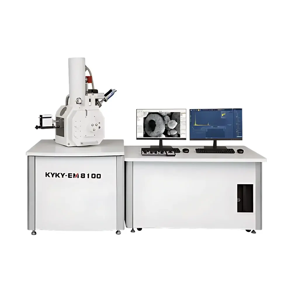
KYKY-EM8100 High-Resolution Field-Emission Scanning Electron Microscope
| Brand | KYKY |
|---|---|
| Origin | Beijing, China |
| Manufacturer Type | Original Equipment Manufacturer (OEM) |
| Instrument Type | Floor-Model SEM |
| Electron Gun | Thermal Field-Emission (TFE) |
| SEM Class | High-Resolution Field-Emission SEM |
| Secondary Electron (SE) Resolution | 0.9 nm @ 30 kV |
| Magnification Range | 1×–3,000,000× (optical: 1×–100×) |
| Accelerating Voltage | 0.2–30 kV |
Overview
The KYKY-EM8100 is a high-resolution thermal field-emission scanning electron microscope (FE-SEM) engineered for nanoscale surface characterization across materials science, semiconductor R&D, advanced ceramics, and life sciences applications. Its optical architecture integrates a patented accelerated column design and a low-aberration conical objective lens, enabling stable sub-nanometer imaging performance at low landing energies—critical for beam-sensitive, uncoated, or insulating specimens. Unlike conventional tungsten or cold-field systems, the TFE electron source delivers exceptional brightness (>1×10⁹ A/cm²·sr), high current stability (2,000 h), supporting both high-resolution topographic imaging and quantitative analytical workflows.
Key Features
- Sub-nanometer resolution at 30 kV (0.9 nm SE) and practical low-voltage imaging down to 1 kV (3 nm SE), minimizing charging and radiation damage
- Conical objective lens with minimized spherical and chromatic aberrations, optimized for short working distance operation and large depth of field
- High-current TFE gun delivering probe currents from 1 pA to 20 nA—enabling simultaneous high-SNR imaging and microanalysis
- Automated column alignment, stigmation, focus, and astigmatism correction via real-time feedback algorithms
- Spacious sample chamber (Ø 200 mm × H 120 mm) accommodating standard SEM stubs, 4″ wafers, and custom holders with ±90° tilt and 360° rotation
- Integrated mirror-based optical navigation system (1×–100× magnification) co-registered with the electron optical axis for precise region-of-interest targeting
Sample Compatibility & Compliance
The KYKY-EM8100 supports diverse specimen types—including conductive metals, semiconductors, polymers, biological tissues (critical-point dried or sputter-coated), and ceramic composites—without mandatory conductive coating in many cases, thanks to its low-kV capability and beam deceleration mode. Vacuum architecture maintains <2×10⁻⁷ Pa base pressure (turbo-molecular pumped) and complies with ISO 14644-1 Class 5 cleanroom requirements for column integrity. All operational parameters—including HV settings, detector bias, stage coordinates, and acquisition timestamps—are logged with audit-trail metadata compliant with GLP and FDA 21 CFR Part 11 for regulated environments. Optional EDS, WDS, and EBSD integration follows ASTM E1508 and ISO 16700 standards for elemental quantification and crystallographic analysis.
Software & Data Management
Control and acquisition are managed through KYKY’s proprietary SEM Suite v4.x—a modular, Windows-based platform supporting DICOM-compatible image export, TIFF/RAW binary output, and HDF5 container format for large-volume datasets. The software includes:
- Real-time dual-channel SE/BSE imaging with independent gain, contrast, and dwell time control per detector
- Automated large-area mosaic stitching: auto-grid planning, fiducial-free alignment, and GPU-accelerated blending (up to 1,024×1,024 tile matrix)
- AI-assisted particle analysis module trained on >50,000 labeled micrographs; performs automatic scale bar recognition, segmentation, morphology classification (aspect ratio, circularity, convexity, Feret diameter), and statistical reporting (CSV, XLSX, PDF)
- Dimensional metrology toolkit: calibrated linear, angular, radial, and polygonal measurements with uncertainty propagation per ISO/IEC 17025 guidelines
- Remote access via TLS-secured API for integration into lab automation frameworks (e.g., LabVIEW, Python pySEM)
Applications
The KYKY-EM8100 serves as a foundational platform for:
- Nanofabrication process control: high-fidelity inspection of lithographic patterns, etch profiles, and thin-film uniformity in MEMS/NEMS development
- Materials failure analysis: fracture surface mapping, inclusion identification, and grain boundary characterization in alloys and composites
- Life science ultrastructure: collagen fibril periodicity, exosome morphology, and mineralized tissue ultrastructure without heavy-metal staining
- In situ and correlative workflows: vacuum-integrated transfer modules enable sequential SEM/FIB-SEM/TEM sample routing under ≤10⁻⁶ Pa conditions
- Time-resolved studies: laser-coupled ultrafast configuration supports pump-probe experiments with temporal resolution down to 10 ps (requires optional femtosecond laser interface)
FAQ
What vacuum level does the KYKY-EM8100 maintain during operation?
The system achieves a base pressure of ≤2×10⁻⁷ Pa using a dual-stage turbo-molecular pumping station with ion getter backup, ensuring long-term emission stability and minimal hydrocarbon contamination.
Is the instrument compatible with third-party EDS or EBSD detectors?
Yes—standard Bruker, EDAX, and Oxford Instruments detectors integrate via IEEE 1394 or PCIe interfaces; full spectral calibration and phase mapping are supported within SEM Suite.
Can the KYKY-EM8100 perform electron beam lithography (EBL)?
An optional EBL add-on module provides vector-scan pattern generation, beam blanking latency <100 ns, and dose-controlled exposure with real-time secondary electron feedback—achieving 15 nm line width fidelity on PMMA resist.
Does the software support automated batch acquisition for quality control?
Yes—scriptable acquisition sequences (Python API) enable unattended multi-sample runs with barcode-triggered metadata tagging, pass/fail thresholding, and auto-alert email notification.
What service and compliance documentation is provided?
Each unit ships with Factory Acceptance Test (FAT) report, ISO 17025-accredited calibration certificate for magnification and acceleration voltage, and full traceability documentation aligned with IEC 61000-4 EMC directives.


