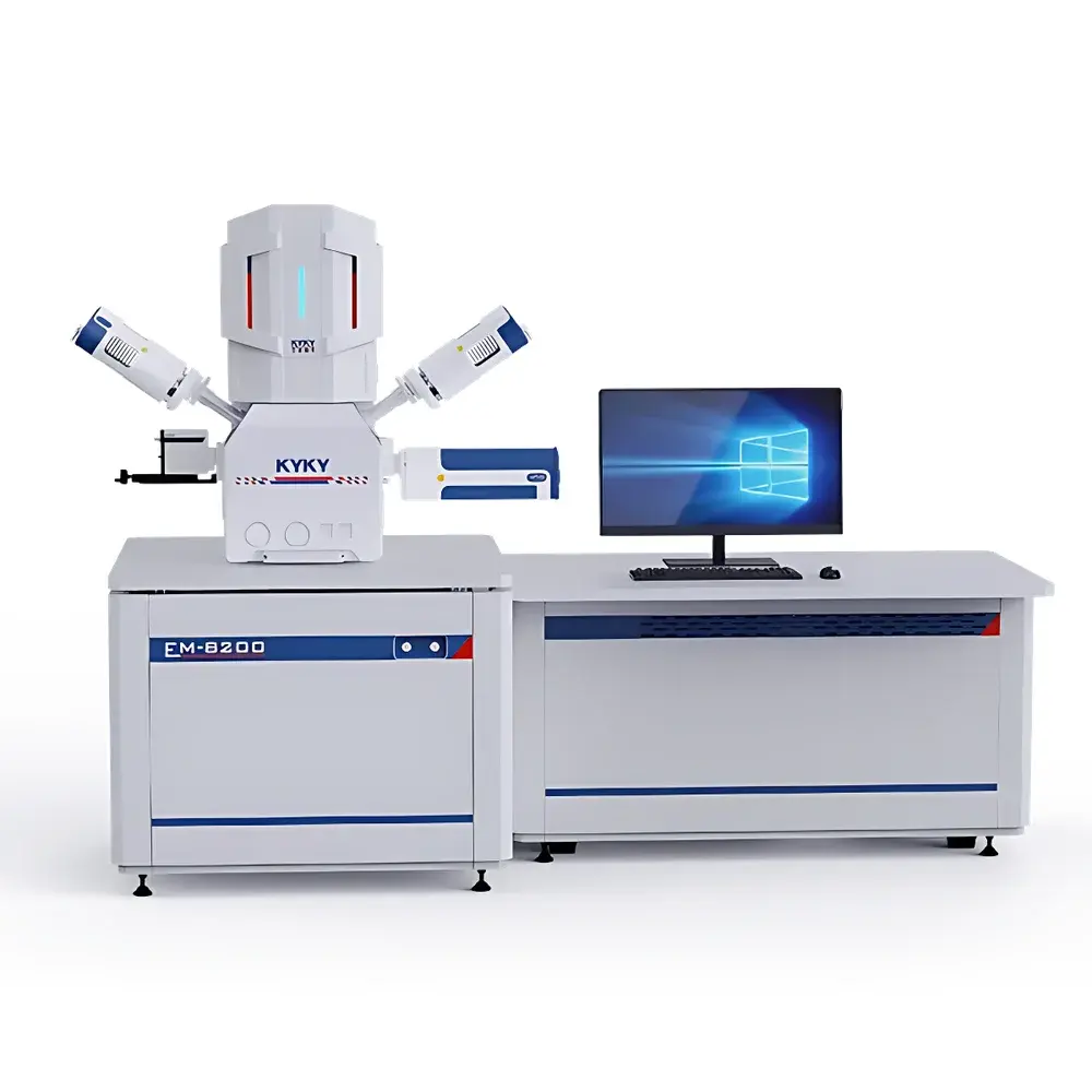
KYKY-EM8200 Ultra-High-Resolution Field Emission Scanning Electron Microscope
| Brand | KYKY |
|---|---|
| Origin | Beijing, China |
| Manufacturer Type | Direct Manufacturer |
| Instrument Type | Floor-Standing SEM |
| Electron Gun | Thermal Field Emission |
| SEM Class | Ultra-High-Resolution Field Emission |
| Secondary Electron Resolution | 0.8 nm @ 15 kV, 1.5 nm @ 1 kV |
| Magnification Range | 1×–3,000,000× (electronic), 1×–100× (optical) |
| Accelerating Voltage | 0.2–30 kV |
Overview
The KYKY-EM8200 is an ultra-high-resolution field emission scanning electron microscope (FE-SEM) engineered for nanoscale structural and compositional characterization in demanding research and industrial environments. Built upon a thermally assisted field emission electron source and a fully optimized electron optical column—including a low-aberration objective lens, decelerated landing stage, and integrated Inlens secondary electron detector—the system delivers sub-nanometer resolution imaging at both high and low accelerating voltages. Its design adheres to core principles of electron optics: minimizing spherical and chromatic aberrations through electromagnetic lens optimization, enabling stable beam formation across the full 0.2–30 kV acceleration range. The instrument supports multi-signal detection (SE, BSE, CL), large-area automated imaging, quantitative morphometric analysis, and advanced in situ functional extensions—making it suitable for applications in semiconductor metrology, battery materials R&D, catalysis, thin-film quality assessment, and nanofabrication process development.
Key Features
- Thermal field emission electron gun with high brightness (>1 × 10⁹ A/cm²·sr) and long-term emission stability under UHV conditions (base pressure <2 × 10⁻⁸ Pa)
- Decelerated sample stage architecture enabling high-resolution imaging at low landing energies (≤1 kV) without compromising signal-to-noise ratio
- Low-aberration immersion-type objective lens with active stigmator and dynamic focus compensation
- Dual-channel real-time imaging: simultaneous acquisition of secondary electron (SE) and backscattered electron (BSE) signals with independent gain/contrast control
- Integrated Inlens SE detector positioned within the objective lens bore for maximum collection efficiency and surface sensitivity
- Motorized retractable BSE detector with atomic number (Z)-dependent contrast enhancement and optional solid-angle optimization
- Optical navigation system with coaxial CCD camera (10×–100× optical zoom) for rapid region-of-interest localization and stage coordination
- Landing beam current monitoring with real-time feedback for consistent imaging conditions across variable kV and working distance settings
Sample Compatibility & Compliance
The KYKY-EM8200 accommodates standard 3-inch (76 mm) and 4-inch (100 mm) diameter wafers, bulk specimens up to 100 mm in diameter and 50 mm in height, and TEM grid holders via optional stages. It supports conductive, semi-conductive, and non-conductive samples—with integrated low-vacuum mode (down to 10 Pa) and optional sputter coater integration for charge mitigation. The system complies with IEC 61000-6-2 (EMC immunity) and IEC 61000-6-4 (EMC emissions) standards. Software operation supports audit trail logging per GLP/GMP requirements, and data export formats (TIFF, BMP, CSV, HDF5) are compatible with third-party analysis platforms used in ISO/IEC 17025-accredited laboratories. All vacuum interlocks and emergency stop circuits meet CE machinery directive (2006/42/EC) specifications.
Software & Data Management
The proprietary SEMControl Suite provides unified control of beam parameters, stage movement, signal acquisition, and post-processing workflows. Key modules include: AutoStitch (automated large-area mosaic acquisition with sub-pixel registration and real-time preview), ParticleAnalyzer (deep learning–enhanced particle segmentation, size distribution fitting, and morphology parameter extraction—e.g., Feret diameter, aspect ratio, circularity, convexity), and MetrologyTool (calibrated distance, angle, radius, and line-profile measurements with traceable scale bar validation). Raw image metadata (kV, WD, dwell time, pixel size, detector configuration) is embedded in TIFF headers. Data management supports hierarchical project folders, user-defined annotation tags, and export to LIMS-compatible XML schemas. Optional FDA 21 CFR Part 11-compliant electronic signature and role-based access control packages are available for regulated environments.
Applications
- Semiconductor device inspection: critical dimension (CD) measurement on finFETs, gate-all-around (GAA) structures, and EUV lithography resist profiles
- Battery electrode microstructure analysis: NMC, LFP, and silicon-anode particle morphology, crack propagation mapping, and SEI layer thickness estimation
- Thin-film quality evaluation: grain size distribution, columnar growth orientation, and interface roughness quantification in PVD/CVD-deposited layers
- Nanomaterial characterization: carbon nanotube alignment, quantum dot dispersion homogeneity, and MOF crystal facet exposure analysis
- In situ functional extensions: electron beam lithography (EBL) patterning with ≤5 nm spot size and 15 nm linewidth fidelity; vacuum-integrated transfer for air-sensitive samples; pump-probe laser coupling for ultrafast electron dynamics studies
FAQ
What vacuum level is maintained in the electron column during operation?
The electron optical column operates at a base pressure better than 2 × 10⁻⁸ Pa, achieved via a combination of turbomolecular pumping and ion gettering. The specimen chamber maintains ≤5 × 10⁻⁶ Pa during standard high-vacuum imaging.
Is the system compatible with energy-dispersive X-ray spectroscopy (EDS)?
Yes—the instrument features standardized detector mounting interfaces (ISO-KF 63) and electrical feedthroughs for OEM or third-party EDS systems. Integration requires mechanical alignment verification and software handshake protocol configuration.
Can the KYKY-EM8200 perform automated particle analysis on non-uniform substrates?
Yes—ParticleAnalyzer employs adaptive thresholding, multi-scale edge detection, and CNN-based classification to segment particles even on textured or low-contrast backgrounds. Scale bar auto-recognition is validated against NIST-traceable calibration standards.
Does the system support remote operation and monitoring?
Remote desktop access via TLS-encrypted VNC is supported. Full operational control—including stage navigation, beam alignment, and acquisition—is available over LAN/WAN with configurable user permissions and session logging.
What is the typical service response time for technical support in international markets?
KYKY provides Tier-2 engineering support via regional partners in North America, Europe, and APAC. On-site service dispatch is scheduled within 5 business days following validated fault diagnosis and parts availability confirmation.


