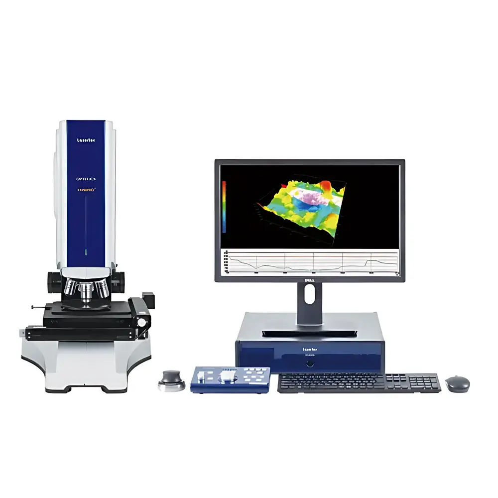
Lasertec HYBRID L7 Confocal Microscope
| Brand | Lasertec |
|---|---|
| Origin | Japan |
| Model | HYBRID L7 |
| Type | Laser Scanning Confocal Microscope with Hybrid Optical & Interferometric Detection |
| Application Domain | Semiconductor Process Metrology, 3D Surface Topography, Thin-Film Thickness Measurement, Microstructure Inspection |
Overview
The Lasertec HYBRID L7 is a high-precision, research-grade confocal microscope engineered for nanoscale metrology in semiconductor fabrication, advanced packaging, and micro-optics development. Unlike conventional widefield or basic confocal systems, the HYBRID L7 integrates dual-path optical architecture—combining laser scanning confocal imaging with white-light interferometry—to deliver simultaneous high-resolution surface topography and sub-nanometer vertical metrology. Its core measurement principle relies on point-by-point axial sectioning via pinhole-confined detection (confocal mode) complemented by coherence scanning interferometry (CSI) for rapid, full-field height mapping. This hybrid approach enables traceable, ISO 25178-compliant 3D surface characterization—including Sa, Sq, Sz, and coplanarity—without requiring sample tilting or multi-acquisition stitching. Designed for integration into R&D labs and pilot production lines, the system meets the stringent stability, repeatability, and environmental robustness requirements of semiconductor process control environments.
Key Features
- Hybrid optical engine: Synchronized confocal + coherence scanning interferometry (CSI) for concurrent high-lateral-resolution imaging and sub-0.5 nm vertical repeatability
- Sub-nanometer axial resolution: Achieves ≤ 0.4 nm height repeatability (σ) over 100 µm range under controlled lab conditions (ISO 25178-6 compliant validation)
- Automated multi-scale 3D profiling: Supports measurement ranges from 100 nm to 10 mm in Z, with lateral resolution down to 120 nm (at 532 nm wavelength)
- Integrated motorized XYZ stage with 100 × 100 mm travel and ±0.1 µm closed-loop positioning accuracy
- Real-time autofocus and auto-focus lock for dynamic measurement during thermal drift or vibration-prone setups
- Modular platform compatible with custom sample holders, probe cards, and inline automation interfaces (SECS/GEM, TCP/IP)
Sample Compatibility & Compliance
The HYBRID L7 accommodates wafers up to 300 mm diameter (with optional chuck), diced dies, bump arrays, lithography masks, and MEMS devices. It supports transparent and reflective substrates—including Si, SiC, GaN, fused silica, and low-k dielectrics—without requiring conductive coating. All measurement algorithms comply with ISO 25178 series (areal surface texture), ASTM E2921 (non-contact 3D profilometry), and SEMI D39 (wafer surface inspection standards). The system architecture supports GLP/GMP-aligned operation: audit trails, user access levels, electronic signatures, and full data integrity per FDA 21 CFR Part 11 when configured with Lasertec’s certified software package.
Software & Data Management
Operated via Lasertec’s proprietary OPTELICS™ software suite, the HYBRID L7 provides scriptable measurement workflows, batch processing for lot-level analysis, and automated report generation (PDF/Excel/CSV). Raw interferometric and confocal datasets are stored in vendor-neutral HDF5 format with embedded metadata (wavelength, objective ID, calibration timestamp, environmental sensor logs). Software includes built-in tools for coplanarity analysis (IPC-7351B reference), bump height distribution histograms, resist pattern edge detection (sub-pixel thresholding), and dicing street inspection with defect classification (chipping, residue, undercut). Data export supports industry-standard formats including STEP AP210, STP, and GD&T-compliant .x3d for CAD integration.
Applications
- Semiconductor front-end: CMP endpoint detection, gate oxide thickness uniformity, trench depth profiling, STI step height
- Advanced packaging: Micro-bump coplanarity (≤ ±1.5 µm spec), solder joint geometry, underfill void detection, TSV opening metrology
- Lithography & etch: Photoresist line width roughness (LWR), mask defect review, hard mask erosion quantification
- Dicing & singulation: Kerf width, chipping depth/width (down to 15 µm lateral resolution), blade wear monitoring
- Thin-film metrology: Single-layer and multi-layer film thickness (50 Å–5 µm), refractive index estimation via spectral reflectance modeling
- MEMS & micro-optics: Mirror flatness, actuator displacement hysteresis, grating pitch verification
FAQ
Does the HYBRID L7 support automated in-line integration with fab AMHS or SECS/GEM protocols?
Yes—optional Ethernet/IP and SECS/GEM interface modules enable direct communication with MES and host equipment controllers.
What is the typical measurement speed for a full 300 mm wafer map at 1 µm lateral sampling?
Using multi-region stitching with adaptive sampling, full-wafer coplanarity mapping takes approximately 12–18 minutes depending on feature density and Z-range settings.
Can the system measure transparent thin films on silicon without ellipsometry?
Yes—the integrated spectral reflectance module (500–1000 nm) enables non-destructive film thickness extraction using interference fringe analysis, validated against reference ellipsometer data.
Is NIST-traceable calibration available for height measurements?
Lasertec offers factory-certified calibration kits (step-height standards, roughness artifacts) with NIST-traceable certificates (NIST SRM 2100 series compatible), delivered with annual recalibration service options.
How is thermal drift compensated during long-duration 3D scans?
The system employs real-time Z-sensor feedback (capacitive metrology) coupled with internal temperature stabilization (±0.1 °C control) and drift-compensated scan path correction algorithms.


