LEED 800 Low-Energy Electron Diffraction System by OCI (Angstrom)
| Brand | Angstrom |
|---|---|
| Origin | USA |
| Manufacturer Type | Authorized Distributor |
| Origin Category | Imported |
| Model | LEED 800 |
| Pricing | Available Upon Request |
Overview
The LEED 800 Low-Energy Electron Diffraction (LEED) System, engineered and distributed globally by OCI since 1998, is a UHV-compatible surface science instrument designed for atomic-scale structural characterization of crystalline surfaces. Operating on the principle of elastic scattering of low-energy electrons (typically 20–500 eV) from periodic surface lattices, the LEED 800 enables real-time observation of surface reconstruction, adsorbate ordering, epitaxial growth dynamics, and phase transitions under ultra-high vacuum (UHV) conditions (≤1×10⁻¹⁰ mbar). Its optical architecture is fully metallic and ceramic—eliminating all polymer-coated wiring, glass-fiber insulation, or epoxy-based feedthroughs—ensuring long-term vacuum integrity and thermal stability during in-situ annealing and dosing experiments.
Key Features
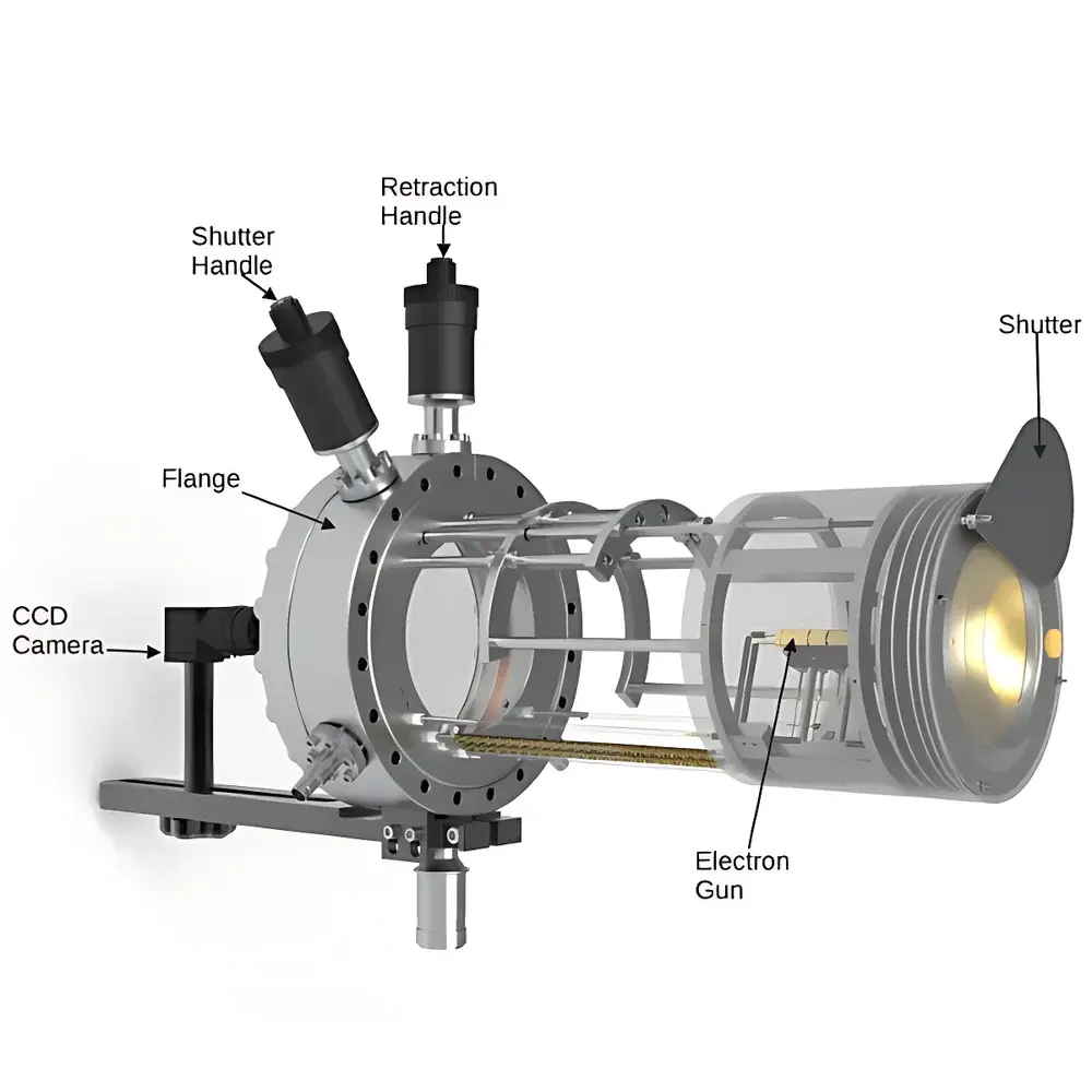
- UHV-optimized electron optics: All components—including electron gun, stigmators, and detector assembly—are constructed from stainless steel, tungsten, and alumina ceramics to maintain base pressure integrity and minimize outgassing.
- Precision 4-grid tungsten electron gun: 1.59 cm (0.625″) diameter source with 103° field-of-view and ≤0.5% energy resolution at 100 eV, enabling high-contrast diffraction pattern acquisition across wide k-space regions.
- Modular, retractable optical column: Standard 2-inch retraction stroke extendable to 4 inches, facilitating integration with multi-technique UHV chambers (e.g., co-aligned AES, XPS, or STM ports).
- Integrated MCP detection: Available in both nA- and pA-sensitivity configurations; includes built-in lock-in amplifier for noise-suppressed signal recovery during low-current surface analysis.
- Flange-integrated viewport and electrical feedthroughs: 6″ and 8″ CF (ConFlat) flange options with direct-line-of-sight viewing and hermetic, all-metal sealed electrical interfaces compliant with ISO-KF and ISO-F standard vacuum practices.
- Compatible auxiliary modules: Optional low-profile mechanical shutters, high-resolution CCD imaging systems (12-bit dynamic range, <10 e⁻ RMS noise), and vendor-neutral control software with scriptable acquisition protocols.
Sample Compatibility & Compliance
The LEED 800 supports conductive and semi-conductive single-crystal samples (e.g., Si(100), Cu(111), Ni(110), MoS₂ monolayers) mounted on standard UHV-compatible sample holders with resistive or electron-beam heating capability (up to 1500 °C). It meets ASTM E1713-21 requirements for surface diffraction instrumentation calibration and is routinely deployed in laboratories adhering to ISO/IEC 17025:2017 quality management systems for surface analysis. All vacuum hardware conforms to ASME B31.3 process piping standards for UHV service, and electrical subsystems comply with IEC 61000-6-3 (EMC emission limits) and IEC 61000-6-2 (immunity testing).
Software & Data Management
Control and data acquisition are managed via OCI’s LEEDSoft™ platform—a Windows-based application supporting real-time pattern capture, reciprocal lattice indexing, intensity vs. energy (I–V) curve generation, and automated symmetry analysis. The software implements audit-trail logging per FDA 21 CFR Part 11 requirements, including user authentication, electronic signatures, and immutable record retention for GLP/GMP-regulated environments. Raw diffraction images are saved in HDF5 format with embedded metadata (beam energy, dwell time, lens voltages, chamber pressure), ensuring traceability and interoperability with third-party analysis tools such as MATLAB, Python (SciPy/NumPy), and commercial surface modeling suites (e.g., CERES, VASP input generators).
Applications
- In-situ monitoring of surface reconstruction during thermal cycling (e.g., Si(111)-7×7 → √3×√3-Ag transition)
- Quantitative determination of adsorbate site occupancy and superstructure formation (CO on Pt(111), O on Ni(100))
- Epitaxial thin-film growth validation in MBE and CVD reactors
- Interface structure analysis of 2D material heterostructures (graphene/h-BN, WSe₂/MoS₂)
- Calibration reference for complementary techniques including Auger Electron Spectroscopy (AES), X-ray Photoelectron Spectroscopy (XPS), and Scanning Tunneling Microscopy (STM)
FAQ
Is the LEED 800 compatible with existing UHV systems from other vendors?
Yes—the system uses industry-standard CF flanges (6″ and 8″ OD), all-metal electrical feedthroughs, and modular mounting interfaces, enabling straightforward integration into chambers from SPECS, Omicron, Focus, or custom-built UHV platforms.
Can the LEED 800 be operated simultaneously with AES or XPS?
Absolutely. Its 4-grid tungsten optics and compact 1.59 cm electron gun footprint allow co-alignment with coaxial or side-mounted AES/XPS analyzers without optical interference or field distortion.
What vacuum compatibility certifications does the LEED 800 carry?
All vacuum-facing components are certified for continuous operation at ≤1×10⁻¹⁰ mbar; no elastomers, epoxies, or polymer-insulated cabling are used—fully compliant with ISO 10110-7 and ASTM F2657-08 for UHV instrumentation.
Does OCI provide installation support and training?
OCI offers on-site commissioning, UHV bakeout supervision, beam alignment verification, and operator training programs covering I–V data acquisition, symmetry analysis, and troubleshooting under variable pressure and temperature conditions.
")