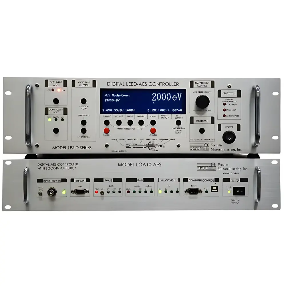
LEED 800 Low-Energy Electron Diffraction System by OCI (Angstrom)
| Brand | Angstrom |
|---|---|
| Origin | USA |
| Manufacturer Type | Authorized Distributor |
| Origin Category | Imported |
| Model | LEED 800 |
| Pricing | Upon Request |
Overview
The LEED 800 Low-Energy Electron Diffraction (LEED) System, engineered and distributed globally by OCI (Angstrom, USA) since 1998, is a high-precision surface science instrument designed for real-time structural characterization of crystalline surfaces under ultra-high vacuum (UHV) conditions. Operating on the principle of elastic scattering of low-energy electrons (typically 20–500 eV), the system generates diffraction patterns that reveal surface periodicity, reconstruction, adsorbate ordering, and domain symmetry with sub-monolayer sensitivity. Its UHV-integrated architecture—featuring all-metal construction, polymer-free insulation, and glass-fiber-free cabling—ensures long-term vacuum integrity (<1×10⁻¹⁰ mbar base pressure achievable) and eliminates outgassing-induced contamination during extended acquisition or in situ annealing experiments. The LEED 800 is routinely deployed in academic surface physics laboratories, national research centers, and industrial R&D facilities focused on catalysis, 2D materials, epitaxial growth monitoring, and thin-film interface engineering.
Key Features
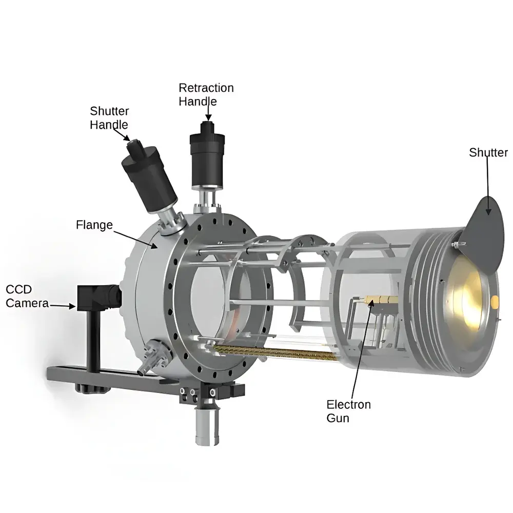
- UHV-compatible optical train: Fully metallic, non-polymeric construction—including tungsten-based 4-grid electron optics—eliminates hydrocarbon contamination and supports bake-out up to 450 °C.
- Precision miniaturized electron gun: 1.59 cm (0.625″) diameter cathode assembly with 103° field-of-view and ≤0.5% energy resolution (ΔE/E) at nominal beam energies.
- Modular, retractable optics: Standard 2-inch retraction depth; optional 4-inch extension for integration with adjacent analytical chambers (e.g., AES, XPS, or MBE systems).
- Dual-mode detection: Compatible with both Faraday cup and microchannel plate (MCP) detectors—supporting pA- and nA-level current measurement with integrated lock-in amplification for noise suppression.
- Integrated flange assembly: Features built-in viewport, feedthroughs for HV, filament bias, and deflection signals—compatible with standard CF-63, CF-100, and ISO-KF vacuum interfaces.
- Low-profile mechanical shutter: Enables precise beam gating for time-resolved LEED studies and dose-controlled surface modification.
Sample Compatibility & Compliance
The LEED 800 accommodates planar, conductive, or semi-conductive samples up to 25 mm in diameter mounted on standard UHV sample holders (e.g., Omicron-style or SPECS-compatible stages). It is fully compatible with common surface preparation techniques—including resistive heating (up to 1200 °C), electron-beam heating, ion sputtering (Ar⁺), and controlled gas dosing (O₂, H₂, CO, NH₃). All components meet ASTM E1758-21 (Standard Guide for UHV Practice) and ISO 14001-compliant manufacturing traceability requirements. The system’s electrical design conforms to IEC 61000-6-3 (EMC emission limits) and IEC 61000-6-2 (immunity standards), ensuring stable operation in multi-instrument UHV clusters. No proprietary software licensing is required for basic operation; firmware adheres to SEMI E10-0218 (Equipment Communications Standard) for interoperability.
Software & Data Management
Control and data acquisition are managed via OCI’s cross-platform LEEDView™ software suite (Windows/Linux/macOS), supporting real-time pattern capture, azimuthal rotation analysis, spot intensity tracking, and dynamic sequence recording (up to 100 fps with MCP mode). Raw diffraction images are saved in HDF5 format with embedded metadata (beam energy, sample temperature, vacuum status, timestamp). The software includes automated calibration routines using known reference lattices (e.g., Cu(100), Si(111)-7×7) and supports export to common scientific formats (TIFF, CSV, CDF). Audit trails, user access logs, and parameter change history comply with GLP and FDA 21 CFR Part 11 requirements when configured with optional electronic signature modules.
Applications
- In situ monitoring of surface reconstructions during molecular beam epitaxy (MBE) and chemical vapor deposition (CVD).
- Quantitative analysis of adsorbate-induced superstructures (e.g., CO on Pt(111), O on Ni(110)).
- Verification of long-range order in self-assembled monolayers (SAMs) and 2D covalent organic frameworks (COFs).
- Time-resolved studies of phase transitions (e.g., (2×1) ↔ c(4×2) on Si(100)) under thermal or reactive gas exposure.
- Complementary use with Auger Electron Spectroscopy (AES) for simultaneous structural and compositional mapping.
FAQ
What vacuum level is required for optimal LEED 800 performance?
Ultra-high vacuum conditions below 5×10⁻¹⁰ mbar are recommended for high signal-to-noise diffraction imaging and to prevent surface contamination during acquisition.
Can the LEED 800 be integrated with an existing UHV surface analysis chamber?
Yes—the system uses standard CF and ISO-KF flanges and provides full electrical and mechanical interface documentation for third-party integration.
Is the electron gun replaceable in the field?
The miniaturized tungsten-filament electron gun is serviceable via front-access ports; replacement kits and alignment procedures are included in the maintenance manual.
Does the system support automated energy-dependent I(V) curve acquisition?
Yes—LEEDView™ enables programmable energy sweeps (20–500 eV, 0.1 eV step) with synchronized intensity logging for quantitative dynamical LEED modeling.
What certifications does the LEED 800 hold for laboratory safety and EMC compliance?
The system carries CE marking per EU Directive 2014/30/EU (EMC) and 2014/35/EU (LVD); full test reports are available upon request for institutional procurement review.