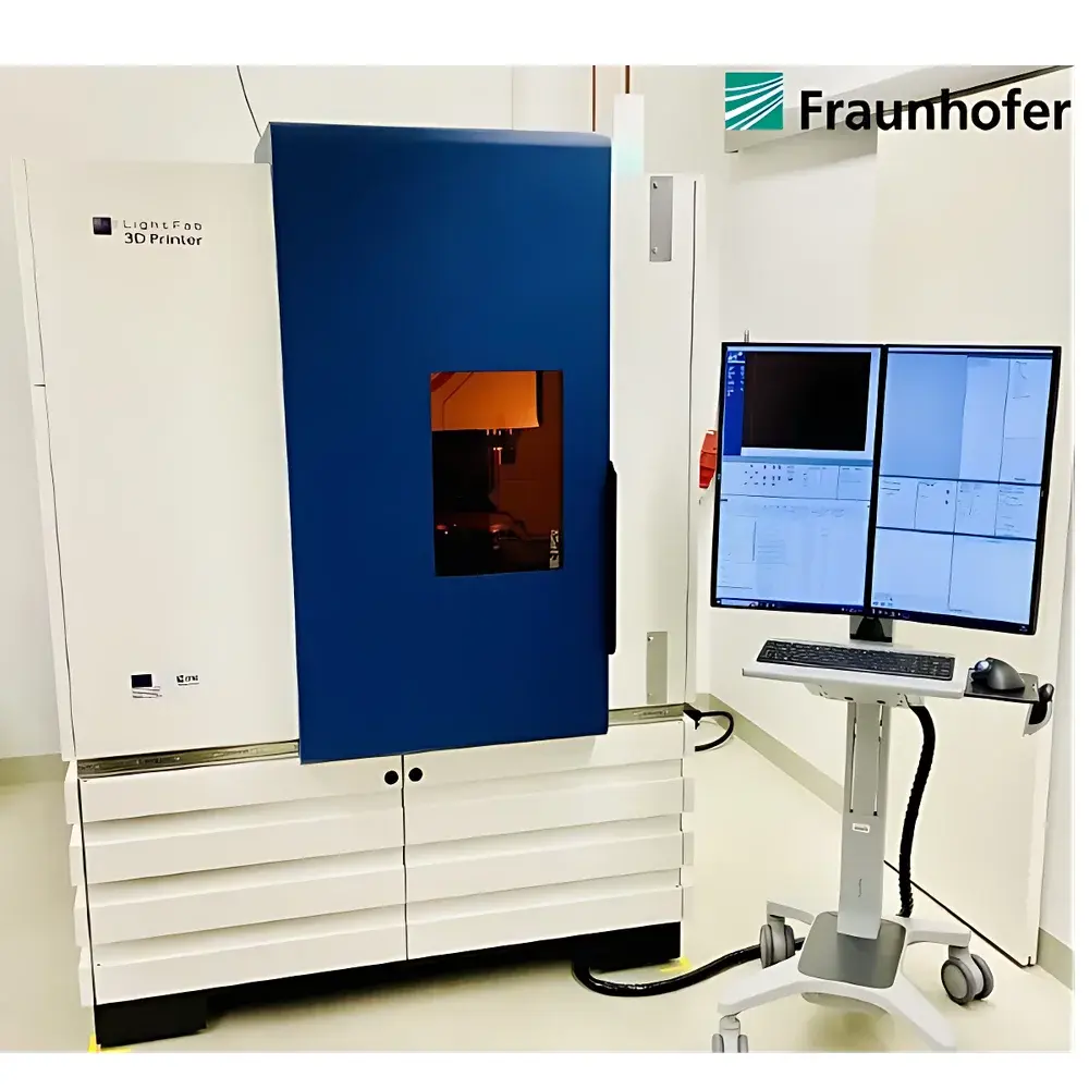
LightFab 3D Femtosecond Laser Micro-Nano Fabrication System for Transparent Glass
| Brand | LightFab |
|---|---|
| Origin | Germany |
| Model | LightFab 3D |
| Technology | Selective Laser-Induced Etching (SLE) |
| Primary Substrate | Fused Silica / Borosilicate Glass |
| Process Type | Two-Step Direct-Write 3D Micromachining (Laser Modification + Wet Chemical Etching) |
| Feature Resolution | Sub-µm Structural Detail |
| Etch Selectivity (Quartz) | >500:1 |
| Application Domain | Integrated Photonics, Microfluidics, MEMS-on-Glass, 3D Waveguide Writing, Hermetic Glass Packaging |
Overview
The LightFab 3D Femtosecond Laser Micro-Nano Fabrication System is a precision-engineered platform designed exclusively for high-fidelity, three-dimensional structuring of optically transparent dielectric materials—primarily fused silica, borosilicate glass, and crystalline quartz. Unlike conventional additive or subtractive 3D printing technologies, the LightFab 3D operates on the principle of Selective Laser-Induced Etching (SLE), a two-step, maskless direct-write process grounded in nonlinear multiphoton absorption. In the first step, ultrashort femtosecond laser pulses (typically <500 fs pulse duration) are tightly focused—achieving diffraction-limited spot sizes below 1 µm—into the bulk of the transparent substrate. This induces highly localized, permanent structural modification without thermal damage, microcracking, or collateral refractive index change in surrounding material. The modified voxels exhibit increased chemical susceptibility to subsequent wet etching, enabling anisotropic, high-aspect-ratio 3D feature definition with sub-micrometer positional accuracy and nanoscale surface roughness (<10 nm RMS). This physics-based approach eliminates the need for photomasks, resist layers, or vacuum environments—making it uniquely suited for rapid prototyping and low-volume fabrication of monolithic glass microsystems.
Key Features
- Femtosecond laser source integrated with high-numerical-aperture (NA > 0.6) objective optics for sub-diffraction 3D voxel placement
- Automated 5-axis motion control (XYZ + tilt + rotation) enabling true volumetric writing in arbitrary orientations
- Real-time beam path calibration and closed-loop focus stabilization for long-duration (>10 hr) exposure consistency
- Native compatibility with standard laboratory-grade HF-based or KOH-based etchants for selective removal of laser-modified regions
- Dedicated SLE process library pre-validated for fused silica, BK7, sapphire, and lithium niobate substrates
- Modular optical design supporting optional integration of in-situ Raman monitoring or interferometric depth profiling
Sample Compatibility & Compliance
The LightFab 3D system is optimized for rigid, amorphous, and single-crystal transparent dielectrics. Verified substrates include Corning Eagle XG, Heraeus Suprasil 300, Schott Borofloat 33, and single-crystal quartz. It supports wafer-scale processing up to Ø150 mm and thicknesses from 100 µm to 10 mm. All hardware and control firmware comply with CE marking requirements (2014/30/EU EMC Directive, 2014/35/EU Low Voltage Directive) and meet IEC 60825-1:2014 Class 4 laser safety standards. Process documentation—including laser parameters, stage trajectories, and etch bath conditions—can be exported in CSV and HDF5 formats to support GLP-compliant recordkeeping and FDA 21 CFR Part 11–aligned audit trails when used with validated third-party LIMS integrations.
Software & Data Management
Control is executed via LightFab’s proprietary SLE Studio software suite, built on a deterministic real-time kernel for synchronized galvo-scanner, piezo-stage, and laser trigger sequencing. The GUI enables interactive 3D CAD import (STL, STEP, IGES), voxel-based path planning with adaptive slicing, and parametric optimization of pulse energy, repetition rate, and scanning velocity per layer. All experimental metadata—including ambient temperature, relative humidity, etchant concentration, and batch lot numbers—is automatically logged alongside raw trajectory data. Export options include ISO 10303-21 (STEP AP242) for geometric traceability and JSON-LD schemas compatible with FAIR data principles. Software updates follow a formal version-controlled release cycle aligned with ISO/IEC 12207.
Applications
- Monolithic 3D microfluidic networks with embedded valves, mixers, and laminar flow splitters in fused silica for lab-on-a-chip diagnostics
- Low-loss, polarization-maintaining 3D waveguides and couplers for quantum photonics and integrated optical interconnects
- Mechanically robust micro-opto-electro-mechanical systems (MOEMS), including gimbaled mirrors and resonant cantilevers fabricated directly inside glass substrates
- Hermetically sealed micro-cavities for pressure, temperature, or biochemical sensing with sub-picoliter volume control
- High-precision micro-molds for nanoimprint lithography and soft lithography master fabrication
- Internal glass-to-glass bonding channels for vacuum-sealed microelectronic packaging
FAQ
What glass types are certified for use with the LightFab 3D system?
Fused silica (Suprasil, Spectrosil), borosilicate (BK7, Borofloat 33), and crystalline quartz are fully characterized; sapphire and lithium niobate are supported under application-specific validation protocols.
Is post-processing thermal annealing required after SLE fabrication?
No—structural stability is achieved intrinsically through the non-thermal nature of femtosecond modification; however, optional annealing at ≤900 °C may be applied to reduce residual stress in thick-section components.
Can the system fabricate free-standing 3D structures within bulk glass?
Yes—by combining volumetric voxel writing with isotropic etchants, self-supporting micro-architectures such as helices, lattices, and gear trains can be realized without sacrificial scaffolds.
Does LightFab provide application support for process transfer to production environments?
Yes—LightFab offers GMP-aligned process qualification packages, including DOE-based parameter mapping, capability studies (Cpk ≥1.33), and IQ/OQ documentation templates for regulated manufacturing sites.
Related Products


