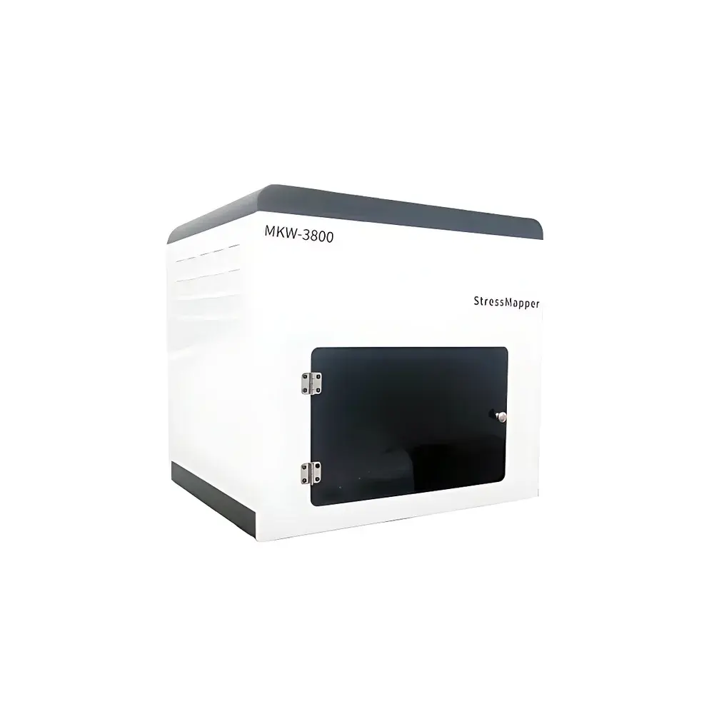
Makeway MKW-3800 Wafer Warpage and Thin Film Stress Measurement System
| Brand | Makeway |
|---|---|
| Model | MKW-3800 |
| Origin | Shanghai, China |
| Measurement Principle | Non-contact structured light reflectometry |
| Sample Diameter | 2–8 inch wafers |
| Sampling Interval | down to 0.1 mm (full-field uniform sampling) |
| Measurement Time | <30 s (for 6-inch wafer, full aperture) |
| Warpage Range | 0.5–5000 µm |
| Warpage Repeatability | ±0.2 µm or ±1% |
| Warpage Accuracy | ±0.5 µm or ±1.5% |
| Stress Range | 1–10,000 MPa |
| Curvature Radius Range | 0.5–10,000 m |
| Curvature Repeatability | <1% (1σ @ 25 m radius) |
| Stress Repeatability | ±1.5 MPa or ±1% |
| Compatible Substrates | Si, GaAs, LiTaO₃, glass, sapphire, InP, SiC, GaN, bonded wafers, patterned wafers, square optical substrates |
| Compatible Films | Si, SiO₂, SiNₓ, Al₂O₃, TiO₂, photoresist, metal films, adhesives, nano-polymeric films, hybrid organic/inorganic films |
| Software | Stress Mapper (real-time acquisition, Stoney equation-based stress calculation, polynomial fitting, spatial filtering, ROI analysis, time-resolved & temperature-dependent stress profiling) |
Overview
The Makeway MKW-3800 Wafer Warpage and Thin Film Stress Measurement System is an engineered metrology platform designed for high-precision, non-contact characterization of mechanical deformation and intrinsic/extrinsic stress in semiconductor and advanced substrate wafers. It operates on the principle of structured light reflectometry—projecting a calibrated fringe pattern onto the wafer surface and reconstructing its topography via triangulation-based phase analysis. This enables full-field, single-shot 3D surface profiling without mechanical scanning, eliminating stage-induced drift and vibration artifacts. The system calculates local curvature radius from the reconstructed height map and applies the modified Stoney equation—accounting for substrate thickness, Poisson’s ratio, and elastic modulus—to derive spatially resolved thin film stress distributions. Unlike point-scan or laser interferometric methods, the MKW-3800 delivers simultaneous warpage and stress mapping across the entire wafer surface, supporting process development, yield enhancement, and failure root-cause analysis in front-end and back-end semiconductor manufacturing.
Key Features
- Full-aperture, non-contact 3D topography acquisition with sub-micron vertical resolution and uniform sampling at intervals as fine as 0.1 mm
- Integrated warpage and thin film stress quantification in a single measurement cycle—no repositioning or mode switching required
- Real-time curvature radius computation and Stoney-based stress mapping with user-configurable material constants (E, ν, tsub, tfilm)
- Support for transparent, semi-transparent, and opaque substrates—including patterned, bonded, and compound semiconductor wafers (Si, GaAs, SiC, GaN, sapphire, glass)
- High-speed acquisition: complete full-field measurement of a 6-inch wafer in under 30 seconds
- Robust architecture optimized for cleanroom integration, with thermal drift compensation and environmental stability monitoring
Sample Compatibility & Compliance
The MKW-3800 accommodates polished and patterned wafers ranging from 2 to 8 inches in diameter, including silicon, gallium arsenide, lithium tantalate, indium phosphide, silicon carbide, gallium nitride, fused silica, and alumina substrates. It supports multi-layer stacks, temporary bonding interfaces, and post-CMP or post-anneal surfaces. Film compatibility spans dielectrics (SiO₂, SiNₓ, Al₂O₃, TiO₂), metals (Al, Cu, Ti, W), polymers (photoresists, BCB, polyimides), adhesives, and hybrid organic-inorganic thin films. All measurements comply with industry-standard definitions of wafer geometry parameters per SEMI MF-1530 and ISO 14407. Stress calculations adhere to ASTM F390-22 (Standard Test Method for Measuring Residual Stress in Thin Films Using the Wafer Curvature Technique), and data traceability supports GLP/GMP-aligned documentation workflows.
Software & Data Management
Stress Mapper software provides a unified interface for instrument control, real-time visualization, and quantitative analysis. It includes automated acquisition sequencing, batch processing for multi-wafer runs, and export of ASCII/CSV-compatible datasets for statistical process control (SPC) integration. Analytical modules include: 3D warpage rendering with color-coded elevation maps; standard wafer metrics (BOW, WARP, TTV, site flatness); region-of-interest (ROI) stress extraction; time-series stress tracking for thermal or aging studies; polynomial surface fitting (up to 12th order); spatial frequency filtering to isolate process-related vs. global deformation modes; and cross-sectional profile slicing at arbitrary angles. Audit trails record operator ID, timestamp, calibration status, and parameter settings—enabling compliance with FDA 21 CFR Part 11 requirements when deployed in regulated environments.
Applications
- Process development and qualification of PVD, CVD, ALD, and spin-coating steps where film stress impacts lithographic fidelity and etch uniformity
- Failure analysis of wafer breakage, delamination, or CMP-induced microcracking linked to residual stress gradients
- Thermal stress modeling validation—measuring stress evolution during rapid thermal annealing (RTA) or cooling cycles
- Quality assurance in MEMS, power electronics, and advanced packaging (e.g., fan-out wafer-level packaging, TSV integration)
- Characterization of low-k dielectric films, high-stress nitride capping layers, and stress-engineered epitaxial structures
- Research into stress relaxation mechanisms in novel 2D materials and heterogeneous integration platforms
FAQ
Does the MKW-3800 require vacuum or inert atmosphere operation?
No—it operates under ambient conditions and is compatible with standard Class 100–1000 cleanroom environments.
Can it measure stress on patterned wafers with high aspect-ratio features?
Yes—structured light reconstruction is insensitive to moderate topography discontinuities; sub-1 µm lateral resolution ensures fidelity even on dense device patterns.
Is temperature-controlled stage support available?
An optional thermostatic chuck (−40 °C to +150 °C) enables in-situ stress-temperature profiling with integrated thermal sensors and closed-loop control.
How is calibration verified?
The system includes NIST-traceable step-height standards and curvature reference plates; daily verification protocols are embedded in Stress Mapper with pass/fail reporting.
What file formats does the software export?
Height maps (.xyz, .stl), stress matrices (.csv, .mat), and report summaries (.pdf, .xlsx) are natively supported; APIs allow direct integration with MES and yield management systems.


