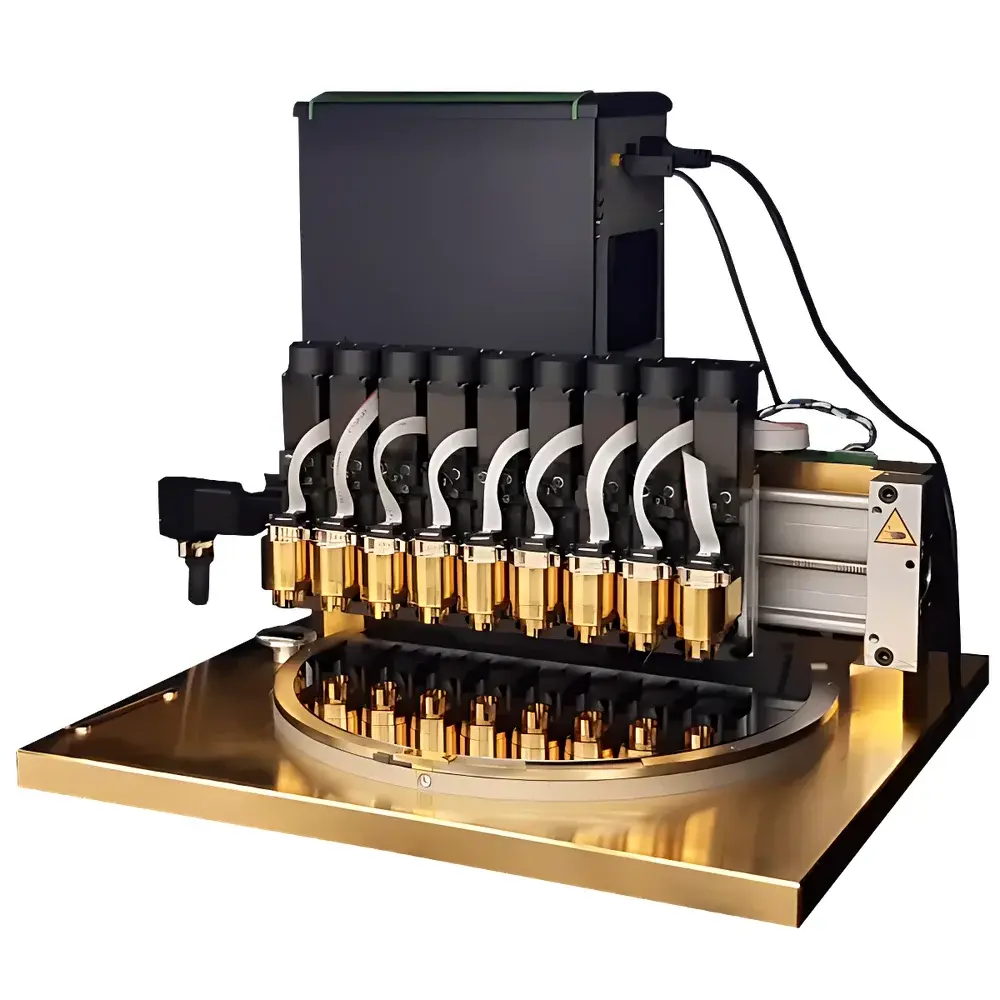
Makeway MKW-KP004 Multi-Probe Scanning Kelvin Probe System
| Brand | Makeway |
|---|---|
| Origin | Shanghai, China |
| Model | MKW-KP004 |
| Probe Count | 9 integrated Kelvin probes |
| Maximum Substrate Size | 300 mm (12-inch) wafers |
| Energy Resolution | < 1 meV |
| Probe Tip Diameter | 1.4 mm (metal) |
| Angular Position Sensing Resolution | 1° |
| X-Axis Motorized Travel | > 100 mm, Positioning Accuracy: ±50 µm |
| Rotational Axis | Motorized silicon wafer stage with integrated optical encoder |
| Dead-Zone Minimization | Optimized for small wafers and wafer fragments |
| Work Function Calibration Reference | Integrated HOPG or Au reference |
| Environmental Monitoring | Onboard USB-connected temperature & humidity sensor |
| Faraday Cage | Fully integrated gold-plated steel enclosure |
| Software Control | Scriptable measurement engine supporting user-defined protocols |
| Data Output | Full-wafer, half-wafer, quarter-wafer, line-scan, and point-mode surface potential maps |
| Compliance Framework | Designed for GLP-aligned lab environments |
Overview
The Makeway MKW-KP004 is a high-precision, multi-probe scanning Kelvin probe (SKP) system engineered for quantitative, non-contact mapping of local surface potential and work function distributions across conductive, semiconductive, and insulating surfaces under ambient or controlled atmospheric conditions. Based on the principle of nullifying the contact potential difference (CPD) between a vibrating metallic reference tip and the sample surface via feedback-controlled DC bias, the MKW-KP004 delivers sub-millielectronvolt (< 1 meV) energy resolution—enabling direct correlation with Fermi-level alignment, interfacial band bending, dipole formation, and charge transfer kinetics. Its modular 9-probe architecture allows parallel acquisition, statistical cross-validation, and spatial redundancy—critical for process monitoring in semiconductor fabrication, thin-film R&D, and functional material screening. The system accommodates substrates up to 300 mm (12-inch) diameter, with motorized X-motion (>100 mm range), precision rotational stage (1° angular resolution), and programmable tip approach control—ensuring reproducible tip–sample gap management without physical contact.
Key Features
- Nine independently addressable, vibration-driven Kelvin probes mounted on a rigid, gold-plated steel frame with full Faraday shielding—minimizing electromagnetic interference and enabling stable low-noise measurements in standard laboratory environments.
- Automated, script-driven data acquisition supporting full-wafer, half-wafer, quarter-wafer, line-scan, and discrete point modes—with integrated dead-zone compensation algorithms for irregular or fragmented substrates.
- Motorized X-axis translation (±50 µm repeatability) coupled with an optically encoded rotational stage (1° resolution) for precise angular registration—essential for anisotropic surface analysis and orientation-dependent work function mapping.
- Onboard temperature and humidity sensors (USB-interfaced) provide real-time environmental metadata synchronized with each measurement—supporting environmental drift correction and long-term stability assessment.
- Integrated calibration references (HOPG and Au) enable in situ work function referencing; all probe tips are standardized at 1.4 mm diameter tungsten or Pt/Ir alloy, compatible with UHV-compatible cleaning protocols.
- Modular software architecture supports Python-based scripting for custom measurement sequences, automated pass/fail thresholding, and integration into fab-level MES or LIMS workflows.
Sample Compatibility & Compliance
The MKW-KP004 accepts planar substrates ranging from 25 mm test coupons to full 300 mm wafers—including Si, GaAs, sapphire, ITO-coated glass, polymer films, and oxidized metal surfaces. No conductive coating or vacuum requirement is necessary, making it suitable for air-stable organic semiconductors, perovskite layers, and biological interfaces. The system’s mechanical design conforms to ISO 14644-1 Class 8 cleanroom compatibility guidelines. While not certified for GMP production use, its data logging architecture supports 21 CFR Part 11–aligned audit trails when deployed with validated third-party software extensions. All electrical subsystems meet CE and RoHS directives; Faraday cage grounding follows IEC 61000-4-3 EMC immunity standards.
Software & Data Management
The native control suite provides real-time CPD visualization, multi-probe synchronization, and batch processing of surface potential maps (output formats: CSV, HDF5, TIFF). Raw voltage traces, tip oscillation harmonics, and environmental metadata are stored with timestamped provenance. Built-in correction routines include thermal drift compensation, tip–sample capacitance normalization, and geometric overlap correction across adjacent probe footprints. For regulated environments, optional add-ons enable electronic signature capture, role-based access control, and encrypted database archiving compliant with ISO/IEC 17025 documentation requirements.
Applications
The MKW-KP004 serves as a primary tool for surface electrostatic characterization across academia and industry. Key use cases include: work function engineering of transparent electrodes in OLED and PV stacks; mapping of corrosion-induced potential gradients on coated alloys; quantification of charge trapping dynamics in gate dielectrics; evaluation of surface dipole layers in self-assembled monolayers (SAMs); Fermi-level pinning analysis at heterojunction interfaces; and in situ monitoring of ion migration in solid-state battery electrolytes. It is routinely deployed in microelectronics process development labs, photovoltaic materials centers, corrosion science facilities, and nanomaterial synthesis groups—where surface potential serves as a direct proxy for interfacial energetics.
FAQ
Is vacuum operation required?
No—the system operates under ambient atmosphere; optional inert-gas purge kits are available for oxygen/moisture-sensitive samples.
Can the system measure insulating surfaces?
Yes—surface potential is measured capacitively; no surface conductivity is required, though topographic artifacts may require complementary AFM or profilometry.
What reference standards are included?
HOPG (highly oriented pyrolytic graphite) and evaporated Au films are provided as factory-calibrated work function references.
Is remote operation supported?
Yes—Ethernet-enabled control allows secure LAN/WAN access; VNC-based GUI sharing and REST API endpoints support integration with lab automation platforms.
Does the system comply with FDA or ISO regulatory frameworks?
The hardware meets general lab safety and EMC standards; full regulatory compliance (e.g., 21 CFR Part 11, ISO 13485) requires site-specific validation using qualified software extensions and documented SOPs.


