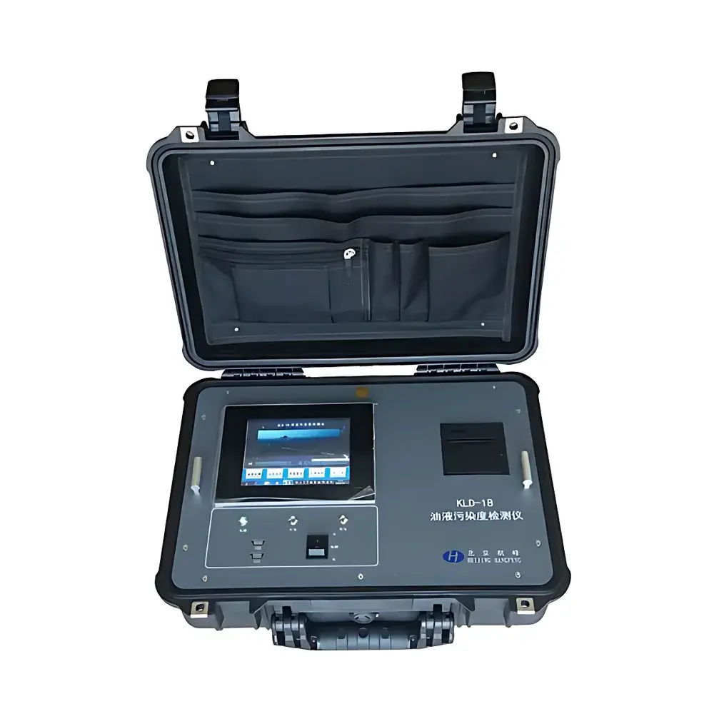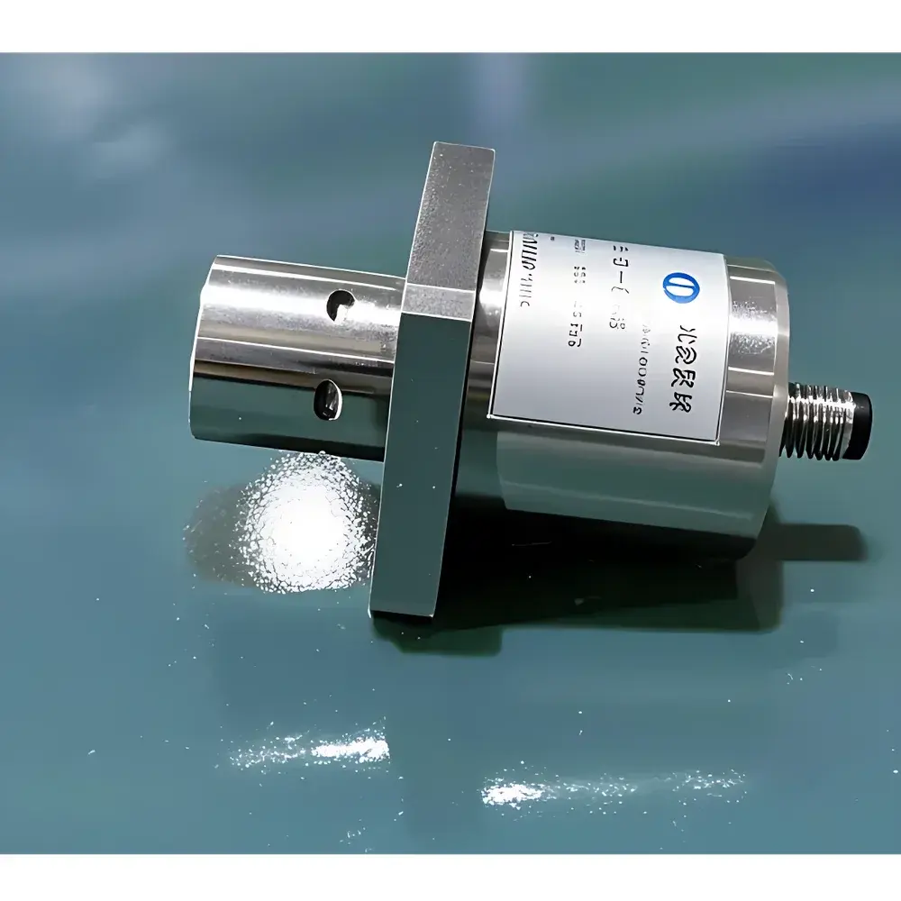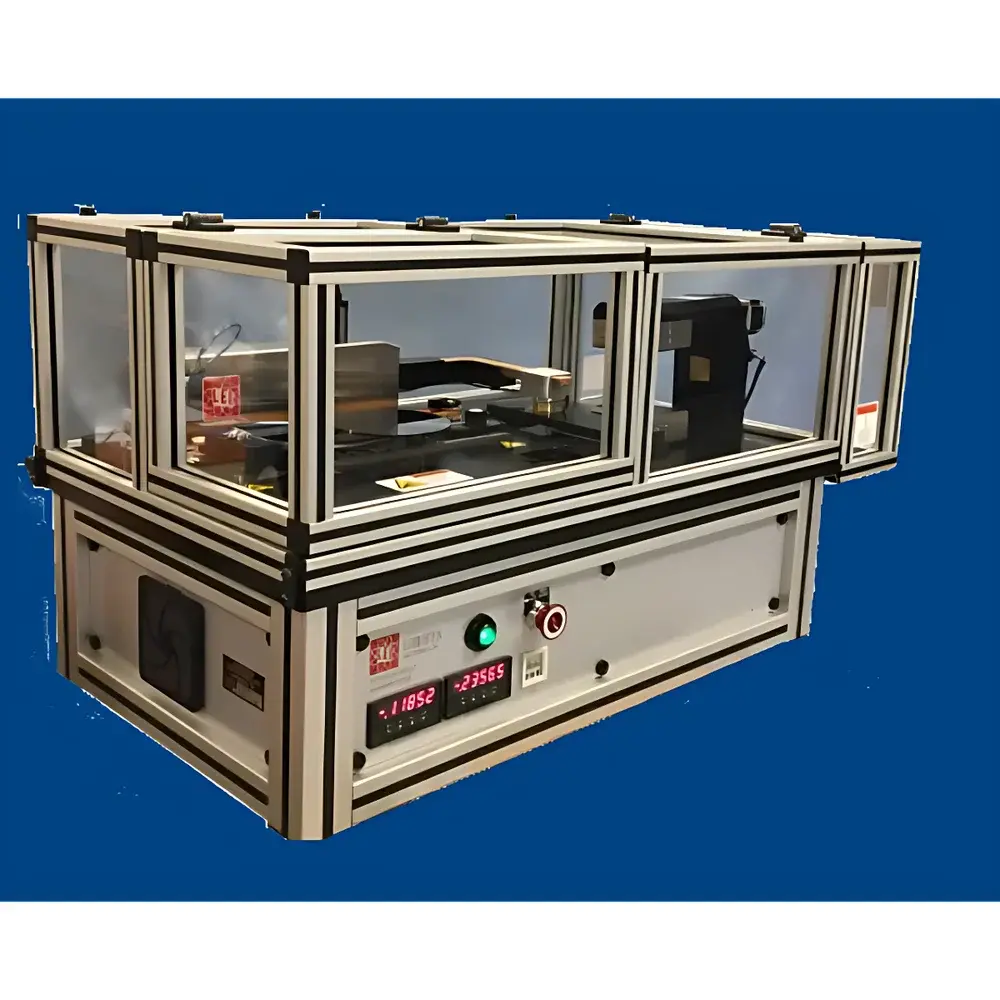
Makeway Model 1600 Non-Contact Microwave Hall Effect Measurement System
| Brand | Makeway |
|---|---|
| Origin | Japan |
| Model | 1600 |
| Instrument Type | Temperature-Variable Hall Effect Tester (Microwave-Based, Non-Contact) |
| Operating Frequency | 10 GHz |
| Current Source Range | 20 mA (for auxiliary calibration & optional DC bias) |
| Sample Diameter Support | 4–8 inch wafers |
| Carrier Mobility Range | 100–3000 cm²/V·s |
| Measurement Modes | Single-Point & Area Mapping |
| Compliance | Designed for ISO/IEC 17025-aligned lab environments |
Overview
The Makeway Model 1600 is a precision microwave-based non-contact Hall effect measurement system engineered for quantitative characterization of two-dimensional charge transport properties in semiconductor thin films and epitaxial layers. Unlike conventional four-point probe or van der Pauw methods, this instrument operates on the principle of microwave perturbation in a waveguide-coupled resonant cavity under controlled magnetic field conditions. At its core, the system employs a low-power 10 GHz microwave source coupled to a rectangular waveguide network capable of exciting and detecting both TE10 (incident/reflected) and TE11 (Hall-induced cross-polarized) modes. When a static magnetic field is applied perpendicular to the sample plane, the Lorentz force induces a transverse voltage—manifested here as a mode-converted TE11 signal—whose amplitude correlates directly with carrier mobility and sheet carrier density. Simultaneously, the magnitude of the TE10 reflection coefficient yields sheet resistance (Rs) with sub-percent uncertainty. This dual-mode detection architecture eliminates physical contact, electrode fabrication, and associated artifacts such as contact resistance, edge effects, or surface damage—making it uniquely suited for process-integrated metrology in R&D and high-mix fab environments.
Key Features
- Non-contact, non-destructive operation: No metal contacts, lithography, or vacuum requirements—enables direct measurement on finished wafers, coated substrates, and fragile 2D materials.
- High-throughput area mapping: Motorized X-Y-Z stage with programmable raster scanning supports automated spatial profiling of Rs, μ, and ns across full 4-inch to 8-inch wafers at ≤50 µm resolution.
- Temperature-variable capability: Integrated cryogenic or heating stage (optional) enables Hall transport analysis from 80 K to 450 K, supporting activation energy extraction and defect-state identification.
- Dual-mode microwave detection: Independent quantification of TE10 reflection (for Rs) and TE11 Hall power (for μ and ns) ensures decoupled, physically grounded parameter extraction.
- Robust electromagnetic shielding: Fully enclosed waveguide chamber with EMI-suppressed RF interlocks meets IEC 61000-4 compliance for stable operation in shared laboratory spaces.
- Modular field integration: Compatible with superconducting magnets (up to 9 T) and electromagnets (up to 2 T), with real-time field synchronization via IEEE-488 GPIB or Ethernet-based SCPI control.
Sample Compatibility & Compliance
The Model 1600 accommodates a broad spectrum of conductive and semi-conductive materials without surface preparation: monolayer and multilayer graphene, exfoliated or CVD-grown TMDs (MoS2, WS2), oxide semiconductors (IGZO, ZnO, NbC, AlN), conductive polymers (PEDOT:PSS), carbon nanotube networks, spin-coated photoresists, colloidal inks, and SiC- or sapphire-based HEMT epiwafers. Powdered samples can be measured in pelletized form using standardized dielectric holders. All measurements adhere to ASTM F76–22 (Standard Test Method for Sheet Resistance of Semiconductor Materials Using Noncontact Microwave Reflectance) and are compatible with ISO/IEC 17025 documentation workflows. Audit trails—including raw S-parameter files, magnetic field logs, temperature timestamps, and operator metadata—are retained per FDA 21 CFR Part 11 requirements when paired with validated software configuration.
Software & Data Management
The system ships with Makeway HallSuite™ v4.2—a Windows-based application developed under IEC 62304 Class B medical software guidelines. It provides real-time visualization of complex S-parameters, automatic calibration against NIST-traceable reference standards (e.g., doped Si wafers), and batch processing of multi-wafer datasets. Export formats include CSV, HDF5, and MATLAB .mat for third-party modeling (e.g., Drude fitting, Boltzmann transport simulations). Role-based user access, electronic signatures, and immutable data archiving support GLP/GMP validation. Raw RF data is stored in vendor-neutral .s2p format, ensuring long-term interoperability with Keysight PathWave, Ansys HFSS, or Python-based analysis pipelines (NumPy, SciPy, scikit-rf).
Applications
- Process development for GaN-on-Si and GaN-on-SiC HEMTs: In-line monitoring of 2DEG sheet density and mobility uniformity across production wafers.
- 2D material transfer optimization: Quantifying doping homogeneity and interfacial scattering in graphene/Cu foil transfers or hBN-encapsulated MoS2.
- Transparent conductor qualification: Rapid screening of ITO, AZO, and AgNW films for display and photovoltaic applications.
- Fundamental transport studies: Extraction of quantum scattering time, effective mass, and valley polarization in topological insulators and twisted bilayer systems.
- Failure analysis labs: Correlating localized mobility degradation with gate dielectric defects or plasma-induced damage in advanced nodes.
FAQ
Does the Model 1600 require sample patterning or electrode deposition?
No. The non-contact microwave method eliminates all need for lithographic processing or metallization.
Can it measure insulating or highly resistive materials?
It is optimized for materials with sheet resistance between 10 Ω/□ and 10 kΩ/□ (carrier density range: ~1×10¹¹–1×1014 cm−2). Ultra-high-resistivity films (>1 MΩ/□) fall outside its dynamic range.
Is magnetic field homogeneity critical for accuracy?
Yes. A uniform field over the measurement spot (<±0.5% variation) is required; the system includes field mapping utilities and recommends use with certified magnet shims or active compensation coils.
How is calibration performed?
Using certified reference wafers traceable to NIST SRM 2135c (doped Si), with automated drift correction during extended mapping runs.
What level of technical support is provided for integration into existing metrology workflows?
Makeway offers on-site installation, IQ/OQ documentation packages, and API-level integration support for SECS/GEM and MES interfaces upon request.