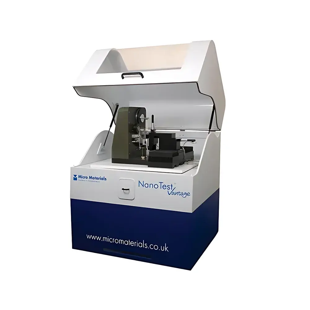
Micro Materials NanoTest Vantage Nanoindentation and Scratch Testing System
| Brand | Micro Materials |
|---|---|
| Origin | United Kingdom |
| Model | NanoTest Vantage |
| Instrument Type | Integrated Nanoindentation & Scratch Tester |
| Maximum Indentation Depth | >10 mm |
| Effective Load Range | 500 mN |
| Load Resolution | 3 nN |
| Displacement Range (XY) | 100 µm × 100 µm |
| Displacement Resolution | 0.002 nm |
| Maximum Friction Force | >250 mN |
| Indenter Types | Diamond, Cubic Boron Nitride (c-BN), Sapphire |
| Thermal Drift | <0.005 nm/s |
Overview
The Micro Materials NanoTest Vantage is a high-precision, modular nanomechanical testing platform engineered for quantitative characterization of mechanical properties at sub-micron length scales. Based on the fundamental principles of quasi-static and dynamic contact mechanics—governed by Oliver–Pharr analysis for indentation and Archard-based models for wear—the system delivers rigorously traceable data on hardness, elastic modulus, fracture toughness, adhesion, creep, fatigue, and tribological behavior. Its dual-actuation architecture combines electromagnetic force application with linear capacitive displacement sensing, enabling simultaneous control of load and displacement across six orders of magnitude—from nano- to micro-newton regimes. Designed for metrology-grade stability, the granite-composite frame, active thermal compensation, and sub-piconewton force resolution make it suitable for ISO 14577 and ASTM E2546 compliant testing in academic research, industrial R&D, and accredited calibration laboratories.
Key Features
- Integrated multi-modal testing: nanoindentation, nanoscratch, nanoscale impact, fretting wear, and high-cycle fatigue—all within a single vacuum-compatible chamber.
- Electromagnetic actuation with 3 nN load resolution and 0.002 nm displacement resolution, ensuring high reproducibility (<1% coefficient of variation) across repeated measurements.
- Modular environmental control: fully independent heating of both sample and indenter up to 850 °C; cryogenic capability down to −20 °C; liquid cell integration for in-situ aqueous or electrolyte testing.
- SPM-grade positioning stage: closed-loop XY scanning range of 100 µm × 100 µm with ≤2 nm positioning accuracy and 99.97% linearity; Z-range of 20 µm for precise topography-coupled mechanical mapping.
- Four-objective optical microscope (×5, ×10, ×20, ×40) with real-time digital magnification up to ×3300 and sub-micron alignment precision for targeted site-specific testing.
- Automated indenter exchange (<60 seconds) supporting diamond, c-BN, and sapphire tips—each calibrated per ISO 14577 Annex B for tip geometry verification.
Sample Compatibility & Compliance
The NanoTest Vantage accommodates diverse specimen geometries—including wafers, thin films, bulk metals, ceramics, polymers, biomaterials, and MEMS devices—within a 50 mm × 100 mm sample stage. Its low-contact-force initiation (<1 µN) prevents surface damage prior to measurement onset, critical for soft or compliant materials. All mechanical test protocols are aligned with international standards: indentation data conforms to ISO 14577 Parts 1–4 (metallic and non-metallic materials); scratch adhesion metrics follow ASTM D7027 and ISO 20502; high-temperature modules satisfy ASTM E220 for thermocouple calibration traceability. The system supports full GLP/GMP audit trails, including electronic signatures, time-stamped raw data logging, and FDA 21 CFR Part 11–compliant software configuration management.
Software & Data Management
NanoWorks™ v6.2 provides a unified interface for experiment design, real-time monitoring, and post-processing. It features automated tip-area function fitting, continuous stiffness measurement (CSM), harmonic analysis for viscoelastic parameter extraction, and spatially resolved property mapping via grid-based indentation arrays. Raw force–displacement curves are stored in HDF5 format with embedded metadata (environmental conditions, calibration certificates, operator ID). Export options include CSV, MATLAB .mat, and NIST-traceable XML schemas. Data integrity is enforced through checksum validation, version-controlled script libraries, and encrypted backup to network-attached storage (NAS) or cloud repositories compliant with ISO/IEC 27001.
Applications
The NanoTest Vantage serves as a primary tool in advanced materials development pipelines. In aerospace, it quantifies thermal barrier coating delamination resistance under cyclic thermal loading. In semiconductor manufacturing, it evaluates interfacial adhesion of low-k dielectrics and Cu diffusion barriers. Biomedical researchers use it to map viscoelastic gradients in cartilage explants or assess osseointegration kinetics of Ti-6Al-4V implants. Thin-film photovoltaic developers rely on its high-temperature scratch module to simulate long-term degradation of perovskite layers. Within fuel cell R&D, it characterizes proton exchange membrane creep compliance under humidified, elevated-temperature conditions—directly informing lifetime modeling and stack design.
FAQ
What standards does the NanoTest Vantage comply with for nanoindentation testing?
It fully satisfies ISO 14577-1 to -4 and ASTM E2546 for instrumented indentation testing, including tip calibration, environmental control validation, and uncertainty budgeting.
Can the system perform tests in aggressive chemical environments?
Yes—optional inert-gas purged or vacuum chambers (10−6 mbar) enable corrosion-resistant testing; liquid cells support pH-controlled electrolytes and biological buffers.
Is remote operation supported for multi-user lab environments?
The NanoWorks software supports concurrent client-server deployment over LAN/WAN, with role-based access control and centralized license management.
How is thermal drift compensated during long-duration creep or fatigue experiments?
Active thermal stabilization—combined with <0.005 nm/s drift specification and real-time thermal drift correction algorithms—ensures sub-nanometer positional fidelity over 24+ hour acquisitions.
Does the system integrate with third-party AFM or SEM platforms?
Yes—via standardized API (REST/JSON) and hardware trigger I/O, enabling synchronized correlative nanomechanical-AFM imaging or in-situ SEM nanoindentation workflows.


