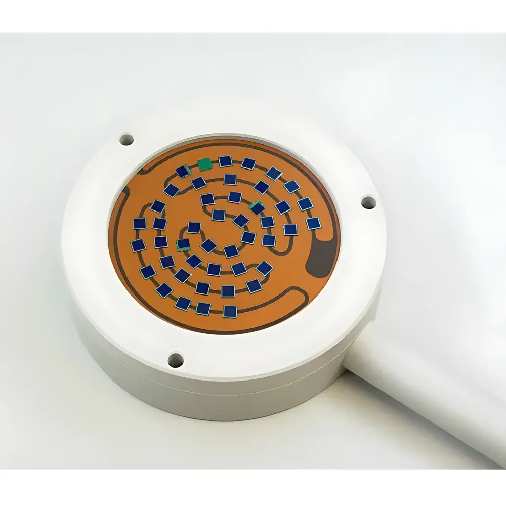
Midas E-chucks Electrostatic Chucks for Semiconductor Wet Etching
| Brand | Midas |
|---|---|
| Origin | Switzerland |
| Type | Electrostatic Chuck (E-chuck) |
| Application | Wafer-level and Die-level Fixturing in Wet Etching & MEMS Processing |
| Compliance | Designed for ISO Class 5–7 cleanroom environments |
| Control Interface | Analog voltage input (0–10 V) or digital RS-485 |
| Holding Force Range | Adjustable up to 0.1–0.8 N/cm² depending on die size and surface condition |
| Substrate Compatibility | Si, SiO₂, SiN, SOI, GaAs, quartz, and patterned MEMS wafers |
| Operating Temperature | Ambient to 80 °C |
| Vacuum Requirement | Optional backside helium cooling interface (compatible with standard wafer chucks) |
| Material | Al₂O₃ ceramic base with embedded bipolar or monopolar electrode architecture |
Overview
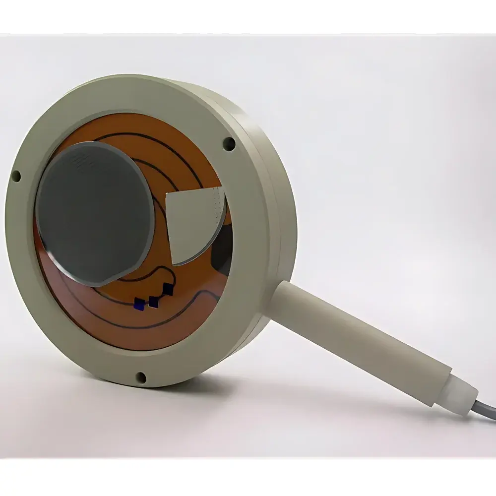
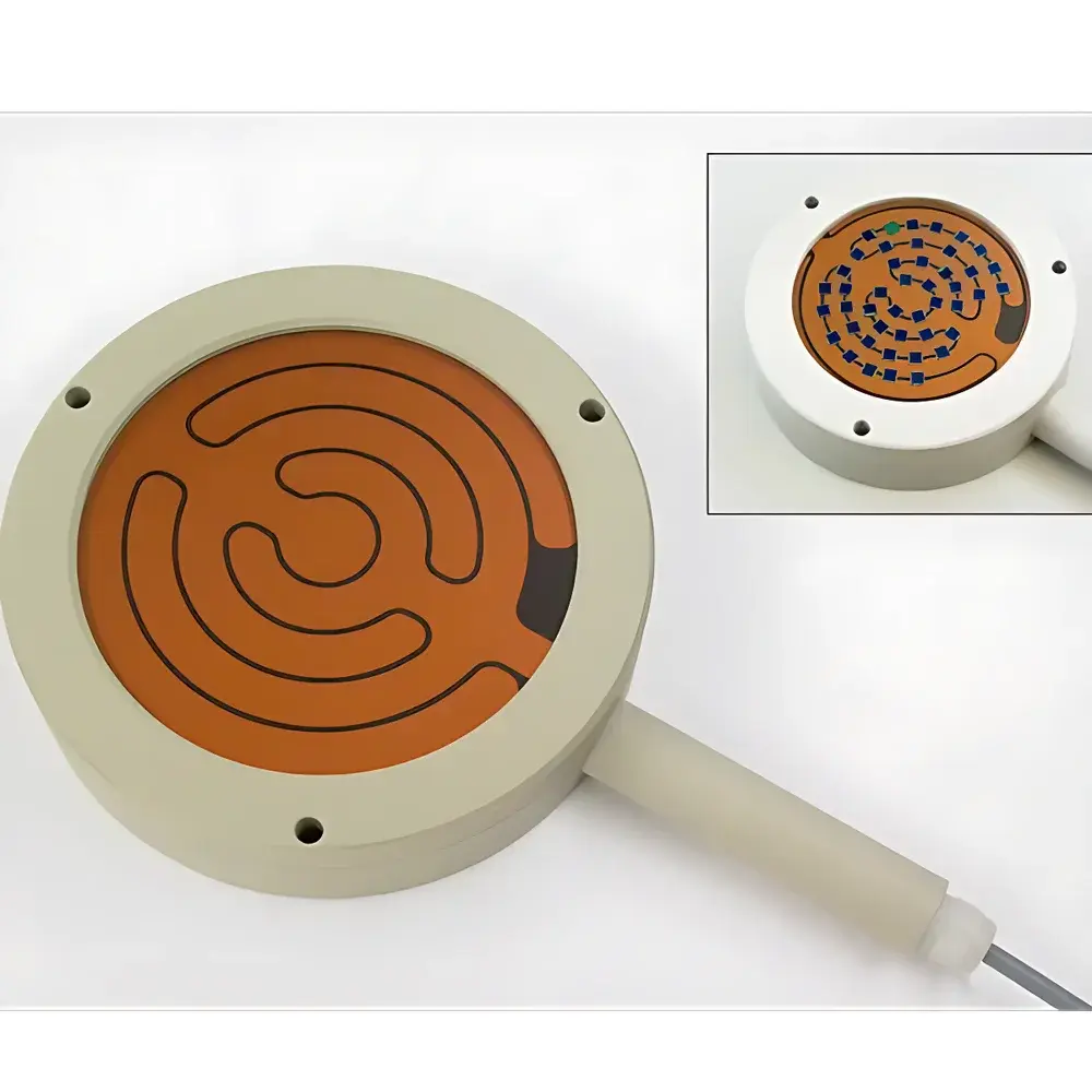
The Midas E-chucks electrostatic chucks are precision-engineered semiconductor process fixtures designed specifically for wet etching, MEMS release, and low-damage die handling in R&D and pilot-line environments. Unlike mechanical clamping or vacuum-based wafer chucks, electrostatic chucks utilize Coulombic and/or Johnsen-Rahbek forces generated by high-voltage DC fields applied across a dielectric-ceramic interface to achieve non-invasive, particle-free substrate immobilization. This principle eliminates physical contact pressure, thermal distortion, and vacuum port contamination—critical advantages when processing fragile, ultra-thin, or pre-patterned MEMS wafers exposed to aggressive chemistries such as HF vapor or buffered oxide etchants. The E-chucks support both full-wafer (100 mm to 200 mm) and partial-wafer or individual die fixation, enabling process flexibility where conventional chucking fails.
Key Features
- Bi-material ceramic construction (Al₂O₃ base with integrated electrode layers) ensures high dielectric strength (>15 kV/mm), low outgassing, and chemical resistance to HF, BOE, KOH, and TMAH solutions.
- Adjustable electrostatic holding force via external DC voltage control (0–10 V analog or RS-485 digital protocol), allowing fine-tuned adhesion for delicate structures without slippage or edge lift.
- No vacuum lines or O-rings required—eliminates risk of liquid ingress, bubble formation, or pump-induced vibration during immersion or spray etching steps.
- Compatible with standard wet bench configurations including dip tanks, spin-rinse developers, and vapor-phase etch modules; footprint-optimized for integration into automated cassette-to-cassette platforms.
- Designed for repeatable performance under GLP-compliant lab conditions; electrode aging characteristics documented per IEC 60664-1 insulation coordination standards.
Sample Compatibility & Compliance
Midas E-chucks accommodate bare and patterned substrates ranging from 5 × 5 mm² diced dies to full 200 mm wafers. Surface compatibility includes silicon, fused silica, silicon nitride, gallium arsenide, and SOI wafers with topography up to 50 µm feature height. The chuck surface finish (Ra < 0.2 µm) and flatness tolerance (≤2 µm PV over 100 mm) meet SEMI F28 specifications for electrostatic wafer handling. All units are supplied with CE marking and RoHS 2011/65/EU compliance documentation. For regulated production use, optional audit-ready firmware logs (timestamped voltage application, duration, and fault events) support FDA 21 CFR Part 11 electronic record requirements.
Software & Data Management
Control is managed via the Midas EC-Controller Box, offering local manual operation (toggle switch + potentiometer) and remote programmability through Modbus RTU or ASCII serial commands. The controller supports configurable ramp-up/down profiles to minimize electrostatic transient stress during engagement/disengagement. Integrated self-diagnostic routines monitor electrode continuity, leakage current (<1 µA at rated voltage), and thermal drift compensation. Data logging (via USB-C or Ethernet) captures real-time chuck status, applied voltage, and environmental temperature—exportable in CSV format for traceability in QC reports or DOE analysis.
Applications
- HF vapor-phase release of surface-micromachined MEMS devices without stiction or curling.
- Localized wet etching of cantilevers, comb drives, and microfluidic channels using photomask-aligned droplet dispensing.
- Dice-level etch testing for process window development prior to full-wafer qualification.
- Low-stress bonding alignment where thermal expansion mismatch prohibits vacuum chucks.
- Plasma-assisted wet cleaning sequences requiring simultaneous electrical biasing and liquid exposure.
FAQ
What substrates are compatible with Midas E-chucks?
Silicon, quartz, SiN, GaAs, SOI, and metal-coated wafers — including those with thin-film piezoelectric or ferroelectric layers. Substrates must be electrically insulating or semi-insulating; conductive wafers require backside metallization isolation.
Can the chuck be used in acidic or alkaline baths?
Yes — the Al₂O₃ ceramic body and hermetically sealed electrodes resist immersion in pH 0–14 solutions for durations up to 30 minutes. Long-term exposure to concentrated HF requires periodic surface inspection per ASTM F2194.
Is dechucking reliable after prolonged etch cycles?
Dechucking is achieved by reversing polarity or applying AC nulling pulses; >99.9% release success rate verified across 500+ cycles on 150 mm Si wafers with native oxide surfaces.
Does the system require grounding or ESD protection?
Yes — all units must be connected to facility earth ground per IEC 61000-6-3 EMC requirements; optional grounded Faraday cage mounting kits available for Class 100 cleanrooms.
How is calibration performed?
No field calibration is needed; factory-certified electrode uniformity (±3% force distribution) and voltage linearity (±0.5% FS) are provided with each unit. Annual verification recommended using certified high-impedance voltmeters and force-sensing films (e.g., Tekscan FlexiForce).


