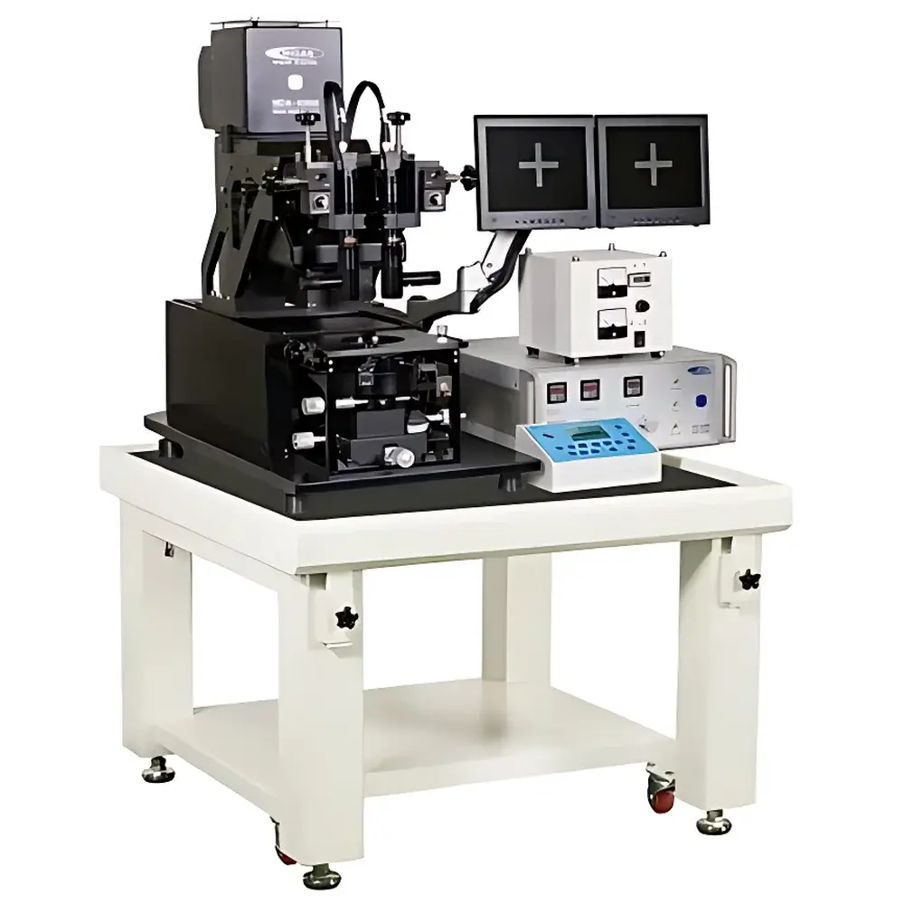
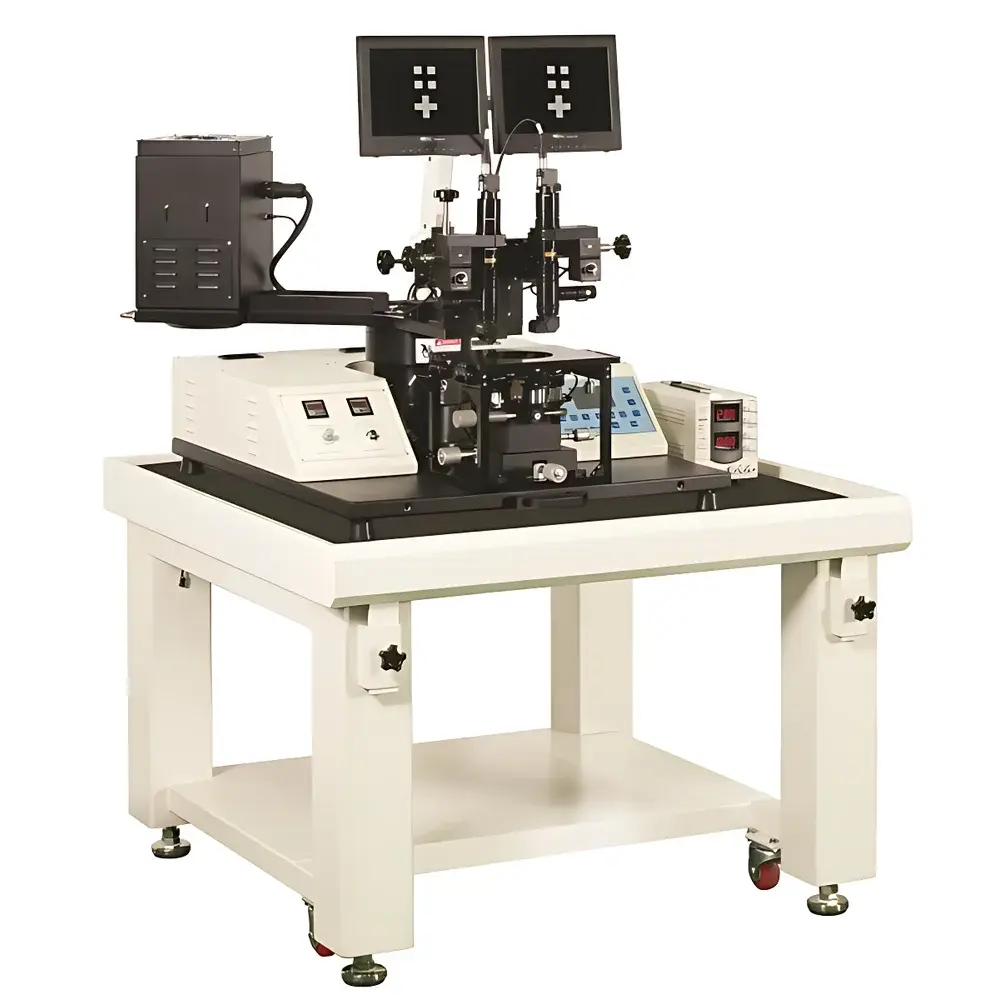
MIDAS MDA-400M Mask Aligner
| Brand | MIDAS |
|---|---|
| Origin | South Korea |
| Model | MDA-400M |
| Exposure Source | Ushio 350W UV Lamp (or optional 365 nm LED, 10,000 h lifetime) |
| Resolution | 1 µm (vacuum/hard contact), 2 µm (soft contact), 5 µm (20 µm gap proximity) |
| Beam Size | 4.25 × 4.25 inch |
| Uniformity | ≤3% (over 4-inch field) |
| Intensity | >30 mW/cm² @ 365 nm |
| Exposure Time | 0.1–999.9 s |
| Alignment Accuracy | ±0.5 µm |
| Stage Travel | X/Y ±10 mm, θ ±5°, Z ±10 mm |
| Approach Step Resolution | 1 µm |
| Microscopy | Dual CCD zoom microscope (80×–480×), 17″ LCD monitor |
| Substrate Compatibility | 2″, 3″, 4″ wafers |
| Mask Size | 4″ and 5″ |
| Vacuum Requirement | < −200 mbar (integrated oil-free pump) |
| CDA | >5 kg/cm² |
| N₂ | >3 kg/cm² |
| Power | 220 V, 15 A, single-phase |
Overview
The MIDAS MDA-400M Mask Aligner is a precision-engineered photolithography tool designed for R&D and low-to-medium volume fabrication in semiconductor, microelectronics, MEMS, bio-MEMS, and nanotechnology laboratories. Operating on the principle of contact/proximity photolithography, the system projects UV radiation—typically at 365 nm (i-line)—through a photomask onto a photosensitive resist-coated substrate. Unlike projection steppers or scanners, the MDA-400M employs a mask-to-wafer alignment architecture that balances resolution, throughput, and operational flexibility. Its optical design ensures high-intensity, spatially uniform irradiation across a 4.25 × 4.25 inch field, enabling reproducible patterning down to 1 µm line/space features under vacuum contact mode on silicon wafers with thin photoresist layers. The instrument supports multiple exposure modes—including vacuum contact, hard contact, soft contact, and programmable proximity gaps up to 20 µm—making it suitable for applications where pattern fidelity, sidewall profile control, and mask longevity must be jointly optimized.
Key Features
- Sub-micron alignment accuracy (±0.5 µm) enabled by dual high-resolution CCD microscopes with 80×–480× continuous zoom and real-time side-by-side image display on a 17″ LCD monitor—eliminating reliance on ocular eyepieces and reducing operator-induced drift.
- Patented wedge error compensation system utilizing pneumatic air-bearing leveling to correct substrate tilt during alignment, critical for uniform resist exposure on warped or non-planar substrates (e.g., glass, quartz, flexible polymers).
- Modular UV exposure engine with interchangeable light sources: standard Ushio 350 W mercury arc lamp (rated for ≥1,000 h) or optional high-stability 365 nm LED module (rated for ≥10,000 h), both delivering >30 mW/cm² intensity at the wafer plane with ≤3% spatial non-uniformity over 4-inch fields.
- Motorized XYZθ alignment stage with 1 µm approach step resolution, ±10 mm lateral travel, ±5° rotational adjustment, and pneumatically actuated coarse/fine proximity control—supporting repeatable, traceable alignment protocols.
- Configurable chuck system compatible with 2″, 3″, and 4″ substrates; custom chucks available for non-standard geometries (e.g., rectangular sensors, biochips, ceramic substrates) and thermal management requirements (e.g., heated/cooled stages).
- Full operational mode flexibility: manual, semi-automatic (user-triggered exposure after alignment), and fully automated sequences (including auto-focus, auto-alignment, multi-field stitching via stage indexing—optional).
Sample Compatibility & Compliance
The MDA-400M accommodates rigid and semi-rigid substrates up to 4 inches in diameter, including silicon, fused silica, sapphire, glass, GaAs, and polymer films (e.g., PI, PET). It accepts standard 4″ and 5″ photomasks with chrome-on-quartz or nickel-on-glass patterns. Vacuum chucking (< −200 mbar, supplied with integrated oil-free pump) ensures stable substrate immobilization without particulate generation. The system meets mechanical and electrical safety requirements per IEC 61000-6-2/6-4 and conforms to CE marking directives. While not certified for ISO Class 5 cleanroom integration out-of-the-box, its sealed optics housing and low-outgassing materials support installation in controlled environments compliant with ISO 14644-1 Class 5–7. All alignment and exposure parameters are logged with timestamps, supporting GLP-compliant documentation workflows.
Software & Data Management
The MDA-400M operates via an embedded industrial PC running a deterministic real-time control kernel. User interaction occurs through a 10.1″ capacitive touchscreen HMI with intuitive icon-driven navigation. Exposure recipes—including dose (mJ/cm²), time (s), gap (µm), lamp intensity (%), and stage coordinates—are stored in encrypted binary files with versioned revision history. Audit trails record operator ID, timestamp, parameter changes, and execution status—fully compliant with FDA 21 CFR Part 11 requirements when paired with network-authenticated login and electronic signature modules (optional). Data export is supported via USB 3.0 and Ethernet (TCP/IP), generating CSV-formatted logs compatible with LIMS and MES platforms. No cloud connectivity or remote vendor access is enabled by default; all firmware updates require physical media verification.
Applications
- R&D-scale fabrication of CMOS-compatible test structures, TFT backplanes, and RF MEMS devices.
- Microfluidic device prototyping using SU-8, AZ, or DJ resist on glass or PDMS substrates.
- Nanopatterning support for plasmonic arrays and metamaterial unit cells via lift-off or etch-transfer processes.
- Biomedical sensor development—including electrode arrays, DNA microarrays, and lab-on-chip interconnects—where sub-5 µm feature definition is required without stepper-level capital investment.
- Education and training in cleanroom processing: widely deployed in university microfabrication facilities (e.g., Nankai University, Institute of Semiconductors CAS, Changchun Institute of Applied Chemistry CAS) for hands-on lithography instruction.
FAQ
What alignment modes does the MDA-400M support?
Vacuum contact, hard contact, soft contact, and proximity (adjustable gap from 5 µm to 20 µm). Proximity mode enables reduced mask wear while maintaining ~5 µm resolution.
Is deep-UV (248 nm or 193 nm) exposure possible?
No—the optical train and lamp housing are optimized for broadband UV (300–400 nm) and i-line (365 nm) operation only. DUV requires dedicated excimer-based systems.
Can the system perform double-sided alignment and exposure?
Yes—via optional IR-transparent substrate holder and dual-wavelength (IR + visible) alignment module, enabling registration of front- and back-side patterns with <1 µm overlay accuracy.
What maintenance is required for the UV lamp or LED source?
Ushio lamps require periodic intensity recalibration every 200 h and replacement at end-of-life (≥1,000 h); LED modules require no scheduled replacement but benefit from annual thermal interface inspection.
Does the system include vacuum and gas supply hardware?
Yes—an oil-free vacuum pump, pressure regulators for CDA and N₂, and all necessary fittings are included in the base configuration.


