Mitaka Micro-Visual Alignment Optical System
| Brand | Mitaka |
|---|---|
| Origin | Japan |
| Model | Micro-Visual Alignment System |
| Camera Sensor Size | 2/3″ |
| Resolution | 2 MP |
| Magnification Range | 0.3×–0.7× |
| Telecentricity | Object-Side Telecentric |
| Illumination | Integrated Coaxial White LED |
| Working Distance | 8 mm (customizable) |
| Alignment Accuracy | 1–10 µm |
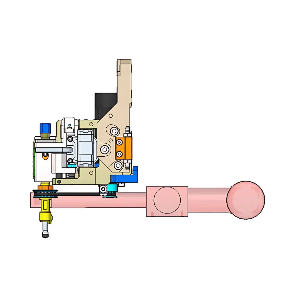
Overview
The Mitaka Micro-Visual Alignment Optical System is a high-precision, object-side telecentric imaging platform engineered for sub-micron registration and alignment verification in advanced semiconductor packaging processes. Built upon the fundamental principle of telecentric imaging—where chief rays are parallel to the optical axis—the system eliminates perspective error and ensures pixel-to-object scale invariance across depth-of-field, critical for repeatable die-to-substrate or bump-to-pad alignment in flip-chip, wafer bonding, and hybrid bonding applications. Unlike conventional macroscopic vision systems, this compact optical architecture integrates coaxial white LED illumination directly into the lens housing, enabling uniform, shadow-free illumination of highly reflective or low-contrast metallized surfaces without external light path interference. Its fixed 8 mm working distance (with optional customization) is optimized for integration into automated bonders, die attach equipment, and inline inspection stations where mechanical clearance and thermal stability are constrained.
Key Features
- Object-side telecentric design ensures negligible parallax and consistent magnification across ±0.5 mm depth of field—essential for accurate overlay metrology on warped wafers or stacked dies.
- 2/3″ format monochrome or color CMOS sensor with 2 MP resolution delivers sufficient sampling density to resolve alignment marks down to 1 µm feature size at 0.3× magnification, supporting ISO 10110-compliant mark detection algorithms.
- Continuously adjustable magnification (0.3× to 0.7×) via precision focus-and-zoom mechanism enables rapid reconfiguration between coarse pre-alignment and fine positional verification without hardware swapping.
- Integrated coaxial white LED illumination provides stable, spectrally neutral output (CCT ≈ 6000 K) with <±3% intensity drift over 8-hour operation—compatible with standard machine vision software SDKs and auto-exposure control loops.
- Compact form factor (<Φ45 mm × 95 mm L) and rigid aluminum alloy housing ensure compatibility with cleanroom-compatible motion stages and minimize thermal drift under 23 ±1 °C ambient conditions.
Sample Compatibility & Compliance
The system is validated for use with silicon wafers (200 mm and 300 mm), organic substrates (ABF, BT), ceramic interposers, and glass carriers. It supports alignment mark types including crosshair, L-shaped fiducials, diffraction gratings, and metal-on-dielectric contrast patterns typical of Cu/Ni/Au UBM stacks. All optical components comply with JIS B 7153 (Japanese Industrial Standard for optical measuring instruments) and meet RoHS Directive 2011/65/EU requirements. The mechanical interface conforms to M36×0.75 metric thread standard for universal mounting on bond tooling flanges. While not intrinsically certified for GMP environments, its sealed optical path and non-outgassing materials support deployment in ISO Class 5 cleanrooms per ISO 14644-1.
Software & Data Management
The optical system operates as a plug-and-play GigE Vision 2.0 compliant device, compatible with HALCON 22.11, OpenCV 4.8+, and Common Vision Blox (CVB) 14.0 APIs. Sub-pixel centroid detection (via moment-based or Gaussian fitting algorithms) achieves repeatability of ≤±0.3 pixels RMS under controlled lighting. Raw image streams include embedded timestamping synchronized to PTPv2 (IEEE 1588-2019) when used with compatible network infrastructure. Audit trails for alignment measurements—including operator ID, timestamp, stage coordinates, and confidence metrics—are exportable in CSV and HDF5 formats to support FDA 21 CFR Part 11 compliance when integrated into validated manufacturing execution systems (MES).
Applications
- Dice placement verification in high-accuracy flip-chip bonder platforms (e.g., F&K Delvotec, Besi, ASM Pacific).
- Real-time overlay error quantification during thermocompression bonding of 2.5D/3D IC stacks.
- In-process inspection of solder paste registration prior to reflow in advanced SiP assembly lines.
- Calibration reference for laser-based alignment sensors in hybrid bonding tools requiring traceable visual ground truth.
- Research-grade metrology for evaluating pattern shift in EUV lithography overlays on test reticles.
FAQ
Is the system compatible with third-party motion controllers?
Yes—standard RS-232 and Ethernet/IP interfaces enable bidirectional communication with Parker, Aerotech, and Newport motion controllers for closed-loop alignment correction.
Can the working distance be extended beyond 8 mm?
Custom configurations up to 25 mm WD are available with recalibrated telecentric optics; lead time increases by 6–8 weeks and requires Zemax-based performance validation.
Does the coaxial illumination support structured light projection?
No—the built-in illumination is diffuse coaxial only; external structured light projectors (e.g., DLP-based) may be coupled via auxiliary C-mount port with optical isolation.
What is the maximum frame rate at full 2 MP resolution?
Up to 60 fps at 8-bit mono mode using GigE Vision streaming; sustained 30 fps achievable with onboard FPGA-based ROI cropping and JPEG compression.
Is calibration documentation provided with shipment?
Each unit ships with NIST-traceable calibration certificate (valid for 12 months) covering magnification linearity, telecentricity deviation (<0.05°), and illumination uniformity (>92% across FOV).


