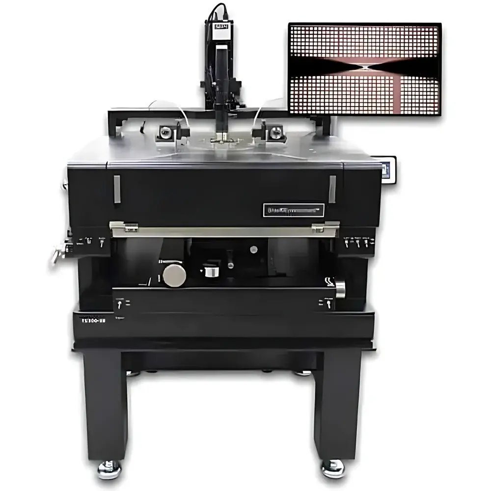
MPI TS200-SE Manual Wafer Probe Station System
| Origin | Germany |
|---|---|
| Manufacturer Type | Authorized Distributor |
| Origin Category | Imported |
| Model | TS200-SE Probe System |
| Price Range | USD 13,500 – 40,500 (FOB) |
| Product Category | Temperature-Controlled Manual Probe Station |
| Operation Mode | Manual |
Overview
The MPI TS200-SE Manual Wafer Probe Station System is a high-precision, thermally regulated platform engineered for on-wafer characterization of semiconductor devices under controlled electromagnetic and environmental conditions. Built upon MPI’s proven mechanical architecture and integrated with ERS thermal management technology, the TS200-SE employs a manual operation paradigm optimized for reproducibility, operator safety, and measurement integrity in R&D, process development, and failure analysis labs. Its core measurement capability relies on direct physical probe-to-device contact within a rigorously shielded environment—enabling low-noise DC, RF/microwave, and high-impedance current measurements down to the femtoampere (fA) range. The system supports wafer-level reliability (WLR), design verification, RF calibration, and high-power device testing across temperature extremes from −60 °C to +300 °C, making it suitable for compound semiconductors (GaN, SiC), advanced CMOS nodes, and MEMS packaging evaluation.
Key Features
- ShielDEnvironment™ fully enclosed EMI/RFI/light-tight chamber with configurable port options: up to 4 RF ports or 8 DC/Kelvin ports for multi-terminal probing
- Three-position chuck lift mechanism (Safe → Contact → Load) with 1 μm repeatability and discrete travel stops at 300 μm separation and 3 mm loading height
- Probe Hover Control™ with selectable hover heights (50 μm, 100 μm, 150 μm) for rapid probe alignment and reduced risk of tip damage
- Air-bearing XY stage with single-hand puck control for smooth, low-friction navigation; augmented by precision 25 × 25 mm XY-Theta micrometer stage for sub-micron positioning
- Motorized Z-axis chuck adjustment (5 mm range, μm-resolution) with 1 mm engraved scale indicator and 20 mm pneumatic lift for fast coarse positioning
- ERS AC3 active air-cooling technology—reduces dry air consumption by 30–50% compared to conventional systems while maintaining stable thermal gradients
- Integrated touchscreen controller mounted at operator eye level for intuitive temperature setpoint management, real-time feedback, and door interlock monitoring
Sample Compatibility & Compliance
The TS200-SE accommodates standard silicon, SOI, GaAs, GaN, and SiC wafers from 100 mm to 200 mm (8-inch) diameter. Optional chucks include coaxial, triaxial, RF-grade (with dual ceramic auxiliary chucks for S-parameter calibration), and ERS AirCool® thermal chucks rated for −60 °C to +300 °C operation. The system meets ISO 14644-1 Class 5 cleanroom compatibility when equipped with filtered air supply. All electrical interfaces comply with IEC 61000-4-3 (radiated immunity) and IEC 61000-4-6 (conducted immunity) standards. For regulated environments, the touchscreen HMI supports audit trail logging and user access levels aligned with GLP and GMP documentation requirements per FDA 21 CFR Part 11 guidelines.
Software & Data Management
While the TS200-SE operates as a hardware platform without embedded firmware-based automation, it is fully compatible with industry-standard instrumentation control frameworks including National Instruments LabVIEW, Keysight PathWave, and Python-based PyVISA drivers. All analog and digital I/O signals—including chuck temperature, door status, lift position, and vacuum interlocks—are accessible via rear-panel BNC and D-sub connectors for external data acquisition and synchronization. Optional MPI ProberLink™ software module enables scriptable macro execution, probe movement logging, and CSV-formatted measurement metadata export—supporting traceability for FA reports and qualification test records.
Applications
- DC parametric characterization (Id-Vg, Id-Vd, leakage current) and compact model extraction
- RF/microwave S-parameter measurements using calibrated on-wafer probes (e.g., GSG, GS configurations)
- Wafer-level reliability stress testing (HTOL, TDDB, HCI) under thermal bias
- Failure analysis workflows including emission microscopy (EMMI), OBIRCH, and laser voltage probing
- High-power device validation (e.g., GaN HEMTs) with simultaneous thermal derating and current monitoring
- MEMS sensor calibration requiring vibration-isolated, low-noise electrostatic actuation
FAQ
What wafer sizes does the TS200-SE support?
Standard configuration supports 100 mm and 200 mm wafers; custom adapters are available for 150 mm substrates.
Is the system compatible with cryogenic probe stations?
No—the TS200-SE is not designed for liquid nitrogen or closed-cycle cryocooler integration; its thermal range is limited to −60 °C to +300 °C using compressed dry air or recirculated gas.
Can the ShielDEnvironment™ be retrofitted onto older MPI probe stations?
ShielDEnvironment™ is mechanically and electrically integrated during factory assembly; field retrofitting is not supported due to chamber sealing, port routing, and EMI gasketing requirements.
Does the system include vacuum chucking capability?
Yes—standard configuration includes a vacuum-compatible chuck with independent vacuum channel routing through the baseplate for seamless integration with external vacuum pumps.
What optical magnification options are available?
MPI offers three microscope options: SuperZoom™ SZ10 (12× optical zoom), MegaZoom™ MZ12 (12× zoom with extended depth of field), and EyeZoom™ EZ10 (10× optical zoom, 90 mm working distance, ≤2 μm resolution).


