MR200 Manual Precision Dicing Saw for Structured Silicon Wafers – Semiconductor Wafer Scribing System
| Origin | Germany |
|---|---|
| Manufacturer Type | Authorized Distributor |
| Origin Category | Imported |
| Model | MR200 |
| Price Range | USD 13,500 – 40,500 (FOB) |
| Maximum Scribing Length | 200 mm |
| Scribing Force Range | 10 g – 130 g |
| Diamond Blade Contact Width | 5 µm – 10 µm |
| Zoom Microscope Magnification | 8× – 40× (continuous, stepless) |
| Optical Resolution at 10× | < 10 µm |
| X/Y Manual Stage Travel | 200 mm × 200 mm |
| Fine Positioning Accuracy | 0.01 mm (X/Y), 0.006° (rotation) |
| Wafer Chuck Diameter | 200 mm (standard), optional 100 mm |
| Vacuum Hold-Down Pressure | < 75 mbar |
| Power Supply | 100–220 V AC, 60 W |
| Dimensions (W×D×H) | 430 mm × 700 mm × 550 mm |
| Weight | ~16 kg |
Overview
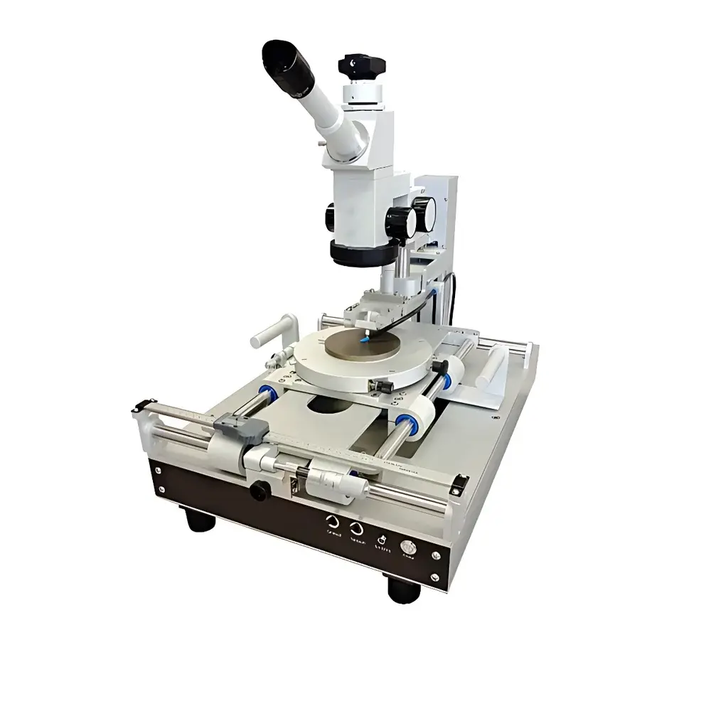
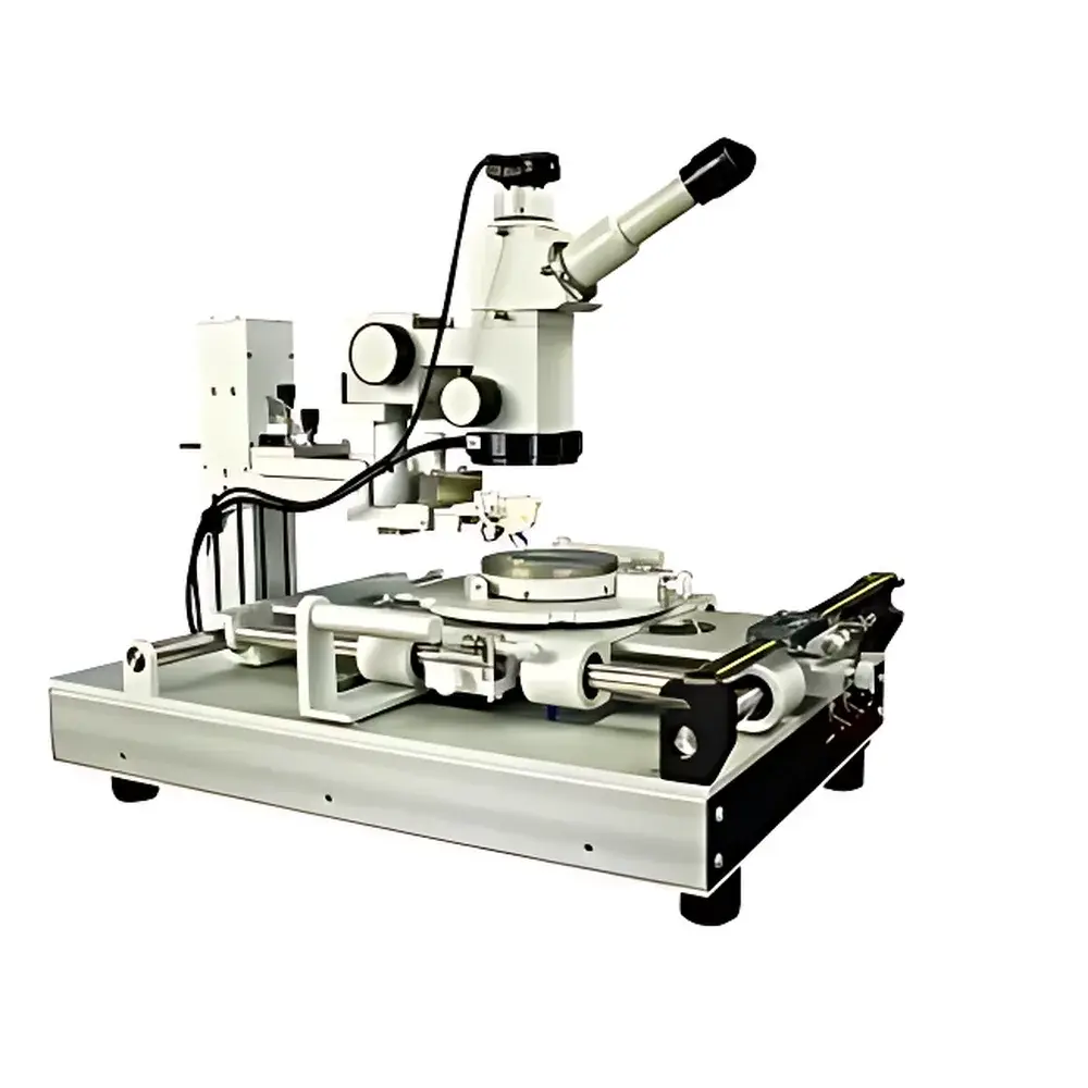
The MR200 Manual Precision Dicing Saw is a high-accuracy scribing instrument engineered for controlled mechanical scoring of structured silicon wafers in semiconductor R&D, prototyping, and low-volume packaging workflows. Unlike full-dicing saws employing rotating diamond blades and coolant systems, the MR200 implements a static diamond-tipped scribe stylus driven by precise manual translation—enabling deterministic, non-destructive surface grooving without material removal or thermal stress. Its core operating principle relies on controlled normal-force indentation followed by lateral shearing motion, producing repeatable micro-grooves with sub-10 µm width and nanoscale depth control. Designed for REM (Resist Etch Mask) preparation, the system supports lithographic alignment fidelity by enabling scribe lines that precisely register to pre-patterned features under optical magnification. The MR200 operates as a benchtop metrology-grade scribing platform—not a production dicer—but delivers laboratory-grade reproducibility essential for process development, failure analysis sample prep, and single-die isolation prior to etch or cleavage.
Key Features
- Robust extruded aluminum frame with vibration-damped base for stable scribing under manual operation
- Stepless zoom microscope (8×–40×) with high-resolution optics and calibrated reticle eyepiece for real-time alignment to edge features, fiducials, or device structures
- Manually actuated X/Y translation stage (200 mm × 200 mm travel) with dual micrometer-driven fine-positioning axes (0.01 mm resolution) and independent 90° vacuum-retained chuck rotation
- Adjustable scribing force (10 g–130 g) via calibrated counterweight mechanism; scribe diamond height, tilt angle, and vertical descent speed are independently tunable
- Teflon-coated vacuum chuck (Ø200 mm standard) with integrated digital angular encoder and mechanical 90° detent stops for orthogonal alignment without vacuum interruption
- Foot-switch-controlled diamond stylus actuation (lower/raise), enabling hands-free scribe initiation while maintaining full manual control over lateral motion
- Integrated LED ring light with adjustable brightness for optimal contrast on reflective Si, GaAs, and compound semiconductor surfaces
- Vacuum particulate extraction port compatible with standard lab filtration systems to prevent redeposition of scribed debris
Sample Compatibility & Compliance
The MR200 accommodates standard silicon wafers (100 mm, 150 mm, 200 mm diameters) across all industry-standard thicknesses (e.g., 275 µm–725 µm), as well as GaAs, SiC, and other brittle semiconductors upon request. Minimum usable sample size is 10 mm × 10 mm. All mechanical and optical components comply with ISO 14644-1 Class 8 cleanroom compatibility requirements when operated in controlled environments. While not certified for GMP manufacturing, the system supports GLP-aligned documentation through optional video capture and image annotation—enabling traceable scribe log generation per sample batch. Alignment repeatability meets ASTM F1725-22 criteria for manual scribing tools used in semiconductor failure analysis labs.
Software & Data Management
The MR200 operates as a hardware-only platform but integrates seamlessly with third-party imaging and measurement software via its optional camera interface kit. This includes a C-mount adapter for industrial CMOS cameras, real-time video streaming to Windows-based workstations, and compatibility with open-source (e.g., ImageJ/Fiji) and commercial (e.g., HALCON, MATLAB Image Processing Toolbox) vision libraries. Optional image processing modules support automated edge detection, line-width quantification, and overlay-based registration error calculation relative to design layout files (GDSII/OASIS). Audit trails—including timestamped video clips, annotated screenshots, and operator ID metadata—can be exported in CSV/PDF formats for internal QA review. No embedded firmware or proprietary OS is present; all data remains fully user-owned and exportable without vendor lock-in.
Applications
- Pre-etch mask definition for REM processes in MEMS and power device fabrication
- Single-die isolation of test chips from probe cards or wafer-level reliability samples
- Controlled crack initiation for cleaving optoelectronic devices (e.g., laser bars, VCSEL arrays)
- Alignment mark scribing for hybrid bonding and heterogeneous integration R&D
- Low-volume prototype dicing where full automation is cost-prohibitive or unnecessary
- Failure analysis sample preparation requiring minimal subsurface damage
FAQ
Is the MR200 suitable for production-line use?
No—the MR200 is explicitly designed for R&D, engineering validation, and low-volume (<50 wafers/month) applications. It lacks automated pattern generation, CNC motion control, or throughput optimization features found in industrial dicing saws.
Can it process non-silicon substrates such as glass or sapphire?
Yes—custom diamond stylus geometries and force calibration profiles are available for brittle dielectrics and wide-bandgap materials; contact technical support for substrate-specific recommendations.
Does the system meet FDA 21 CFR Part 11 requirements?
Not natively—the MR200 has no electronic signature capability or audit trail logging built-in. However, when paired with validated third-party video capture and annotation software under a documented SOP, it may be incorporated into Part 11-compliant workflows.
What maintenance is required for long-term optical performance?
Annual recalibration of the microscope’s magnification scale and reticle alignment is recommended. Diamond stylus replacement intervals depend on usage intensity but typically exceed 500 linear meters of scribing on Si.
Is vacuum pump included with the system?
No—a compatible dry diaphragm vacuum pump (≤75 mbar ultimate pressure, ≥10 L/min flow) must be sourced separately; specifications and mounting interfaces are provided in the installation manual.
Related Products


