Nano analytik AFM Series SmartProbe-Integrated Atomic Force Microscope
| Brand | Nano analytik |
|---|---|
| Origin | Germany |
| Model | AFM Series (SmartProbe Platform) |
| Instrument Type | Atomic Force Microscope |
| Vertical Position Detection Noise | 0.01 nm RMS |
| Maximum Sample Diameter | ≤10 cm |
| Scanner Range (Adeona) | 15 µm × 15 µm × 4 µm |
| Dimensions (Vacuum-Compatible Version) | 140 mm × 100 mm × 60 mm |
| Integrated Actuation & Sensing | Piezoresistive readout + bimaterial excitation on SmartProbe |
| XYZ Nanopositioning Range (Vacuum Variant) | 20 µm × 10 µm × 10 µm |
Overview
The Nano analytik AFM Series is a modular, high-stability atomic force microscope platform engineered for precision nanoscale surface characterization in ambient, liquid, and ultra-high vacuum (UHV) environments. Unlike conventional optical beam-deflection AFMs, this system employs integrated piezoresistive sensing and bimaterial actuation directly embedded within its proprietary SmartProbe cantilever—eliminating laser alignment, photodetector drift, and optical path constraints. The core measurement principle relies on direct electrical transduction of cantilever deflection and resonance dynamics, enabling robust, quantitative force-distance spectroscopy, topographic imaging, and nanomechanical property mapping with sub-angstrom vertical resolution. Designed by engineers and physicists from Technische Universität Ilmenau and co-developed with Analytik Jena AG, the platform emphasizes reproducibility, ease of integration, and compliance-ready architecture for academic labs, industrial R&D centers, and regulated quality control environments.
Key Features
- SmartProbe technology: Monolithic silicon cantilevers integrating piezoresistive sensors and bimaterial thermal actuators—no external optics required.
- Sub-nanometer stability: 0.01 nm RMS vertical detection noise achieved via low-noise analog front-end and active thermal drift compensation.
- Modular scanner architecture: Adeona scanner (15 µm × 15 µm × 4 µm range) for standard operation; optional vacuum-compatible XYZ nanopositioner (20 µm × 10 µm × 10 µm) with UHV-rated materials and feedthroughs.
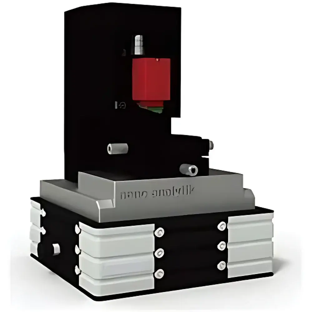
- Compact SEM-integration design: Fully self-contained AFM head (140 × 100 × 60 mm) mounts directly into standard SEM chambers without chamber modification or venting cycles.
- Open hardware/software interface: IEEE 1451.4-compliant transducer metadata, Python/C++ SDK, and LabVIEW drivers support custom automation, closed-loop control, and third-party instrument synchronization.
- Multi-environment compatibility: Validated operation in air, controlled humidity, aqueous buffer solutions, and vacuum down to 10⁻⁷ mbar.
Sample Compatibility & Compliance
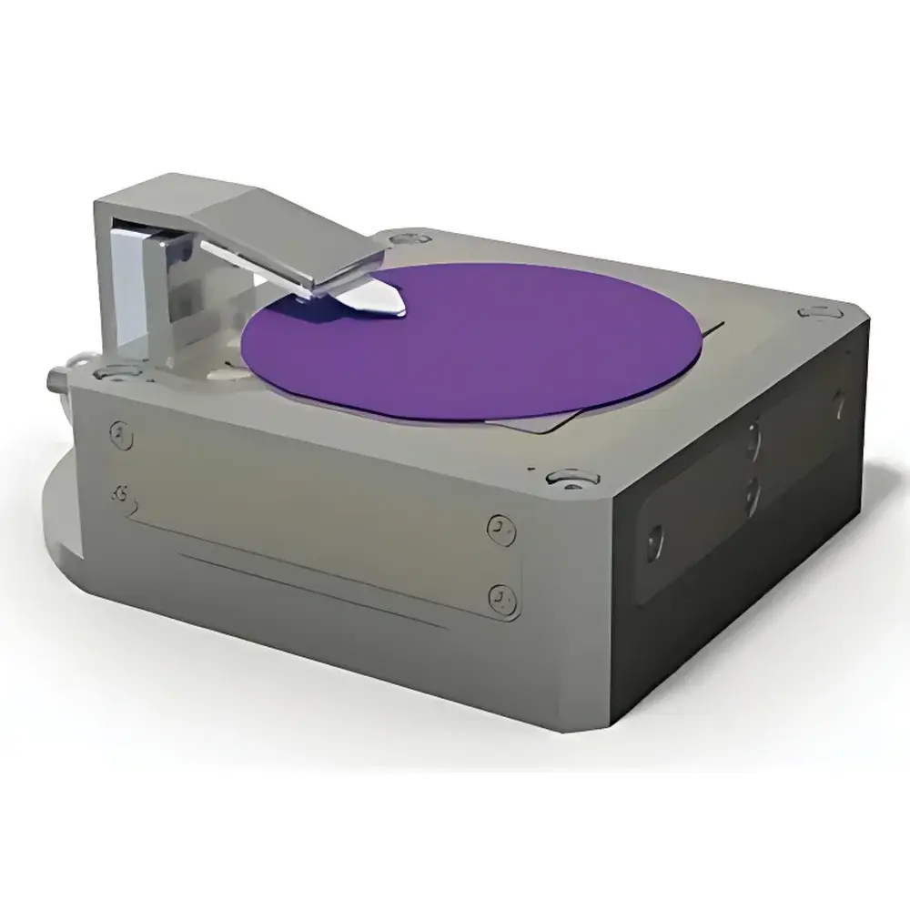
The system accommodates samples up to 10 cm in diameter on a motorized, tilt-adjustable stage. Its non-optical detection scheme ensures insensitivity to sample optical properties—enabling reliable imaging of opaque, highly reflective, or light-absorbing materials including metals, semiconductors, polymers, and biological specimens. All vacuum-capable variants conform to ISO 14644-1 Class 5 cleanroom handling protocols and utilize oxygen-free copper and ceramic insulators to minimize outgassing. Firmware and acquisition software support audit trails, electronic signatures, and configurable user roles—facilitating alignment with GLP, GMP, and FDA 21 CFR Part 11 requirements when deployed in regulated material qualification or biocompatibility testing workflows.
Software & Data Management
Acquisition and analysis are performed using Nano analytik’s AFM Control Suite v4.x—a deterministic real-time application built on a dual-threaded Linux RT kernel. The software provides synchronized multi-channel data logging (up to 16 channels at 2 MHz), automated probe calibration (thermal tune, Sader method), and standardized export formats (HDF5, TIFF, ASCII) compliant with MIAME and FAIR data principles. Built-in modules support quantitative nanomechanics (Young’s modulus, adhesion energy), phase imaging deconvolution, and tip-sample convolution modeling. Raw data files include embedded metadata (probe ID, environmental conditions, calibration timestamps) and are checksum-verified upon write to ensure integrity across long-term storage or cross-lab collaboration.
Applications
- Materials science: Grain boundary mapping in polycrystalline thin films, polymer phase separation analysis, graphene layer counting, and defect quantification in III-V semiconductors.
- Life sciences: In situ imaging of membrane proteins in supported lipid bilayers, mechanical phenotyping of live cells under physiological buffer flow, and fibril stiffness profiling in amyloid aggregates.
- Sensor development: Calibration and functional validation of piezoresistive and capacitive MEMS cantilevers used in biochemical detection platforms.
- Failure analysis: Cross-sectional topography and nanoscale wear assessment of microelectromechanical systems (MEMS) devices post-reliability stress testing.
- Correlative microscopy: Simultaneous SEM-AFM acquisition for structural-electrical property correlation in battery electrode cross-sections and catalyst nanoparticles.
FAQ
Does the system require laser alignment during setup or daily operation?
No—SmartProbe eliminates optical beam deflection entirely. Alignment is reduced to mechanical docking of the probe holder; no iterative laser tuning or photodiode centering is necessary.
Can the AFM operate inside a scanning electron microscope without breaking vacuum?
Yes—the vacuum-compatible variant maintains UHV integrity (≤10⁻⁷ mbar) and integrates via standard CF-40 or KF-40 flanges. No chamber modifications or additional pumping stages are required.
Is probe calibration traceable to national standards?
Yes—thermal noise and Sader methods are implemented per ISO/IEC 17025-accredited procedures. Calibration certificates include uncertainty budgets referenced to PTB (Physikalisch-Technische Bundesanstalt) traceable cantilever spring constants.
What level of technical support is provided for custom software integration?
Nano analytik offers documented C/C++ APIs, Python bindings, and optional on-site SDK training. Remote debugging and firmware-level access are available under NDA for OEM partners and large-scale deployment contracts.
Are there regulatory documentation packages available for GxP environments?
Yes—validated installation qualification (IQ), operational qualification (OQ), and performance qualification (PQ) protocols are supplied as part of the GxP Compliance Package, including risk assessments and change control templates aligned with ICH Q9 and ISO 13485.


