Nano analytik SPL Scanning Probe Lithography System
| Brand | Nano analytik |
|---|---|
| Origin | Germany |
| Model | SPL |
| Instrument Type | Atomic Force Microscope-based Scanning Probe Lithography System |
| Positioning Detection Noise | 0.01 nm (X, Y, Z) |
| Maximum Sample Diameter | 150 mm (6 in) |
| Stage Travel Range | 18 mm × 18 mm (expandable to 150 mm × 150 mm) |
| Minimum Feature Size | 5 nm (verified) |
| Direct-Write Speed | 300 µm/s |
| Overlay Accuracy | < 7 nm |
| Stitching Accuracy | < 10 nm |
| Maximum Writing Area per Field | 200 µm × 200 µm |
| Footprint | 80 cm × 100 cm × 190 cm |
| AFM Imaging Range | 10 µm × 10 µm × 5 µm (expandable to 200 µm × 200 µm) |
| Vertical RMS Noise | 0.01 nm |
| Closed-Loop Scan Linearity | 99.7% |
| Real-Time FPGA Feedback Bandwidth | 8 MHz |
| Data Acquisition Resolution | 16-bit (amplitude/phase) |
| Output Formats | BMP, PNG, JPG, TXT |
Overview
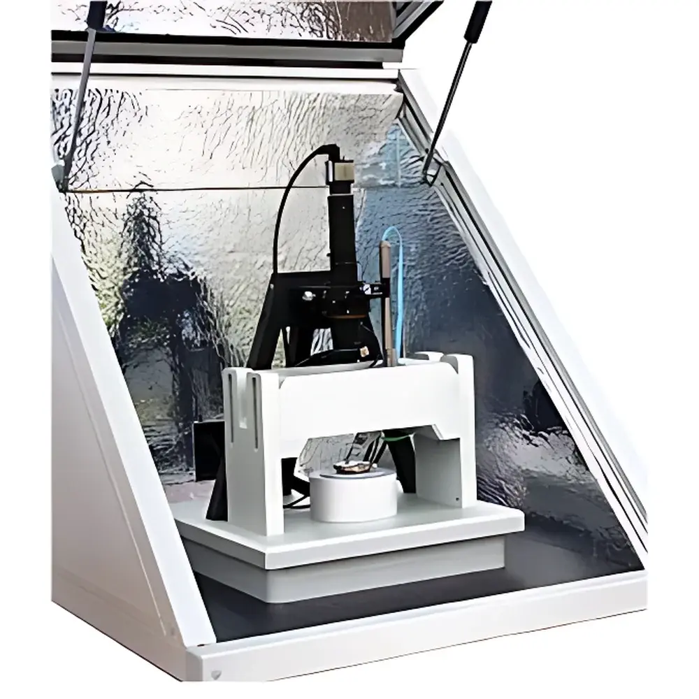
The Nano analytik SPL Scanning Probe Lithography System is a high-precision, AFM-integrated nanofabrication platform engineered for sub-10 nm direct-write lithography under ambient conditions. Unlike conventional electron-beam lithography (EBL) systems that rely on vacuum environments and suffer from proximity effects, the SPL employs a field-emission low-energy electron beam generated at the apex of a conductive scanning probe tip. This configuration eliminates beam broadening and backscattering, enabling true nanoscale patterning without electron-optical column complexity or resist development steps. The system operates on a hybrid principle: combining scanning probe microscopy (SPM) metrology with localized electron-induced surface modification—leveraging the same tip for real-time topographic imaging, precise feature registration, and deterministic nanoscale writing. Its closed-loop architecture ensures traceable positioning across the full operational range, making it suitable for research-grade maskless fabrication, quantum device prototyping, plasmonic nanostructure engineering, and calibration standard generation.
Key Features
- Sub-5 nm resolution lithography verified per ISO/IEC 17025-compliant acceptance testing
- Integrated atomic force microscope functionality with automatic cantilever tuning and laser-free approach control
- Closed-loop XYZ piezoelectric positioning with 0.01 nm sensor resolution and 99.7% scan linearity
- Ambient-atmosphere operation—no vacuum chamber required—reducing infrastructure cost and turnaround time
- Simultaneous positive/negative tone lithography modes; positive-tone process omits developer step
- Mix-and-match overlay capability for alignment to pre-patterned substrates with <7 nm overlay error
- Modular stage design supporting 18 mm × 18 mm standard travel, upgradable to 150 mm × 150 mm for wafer-scale stitching
- Real-time FPGA-based feedback control (8 MHz bandwidth) for dynamic tip-sample interaction compensation
- Multi-tip array compatibility for parallelized throughput scaling (optional configuration)
Sample Compatibility & Compliance
The SPL accommodates standard semiconductor wafers up to 150 mm (6-inch) diameter and supports diverse substrate materials including Si/SiO₂, SiN, HOPG, Au, Pt, and functionalized polymer films. All motion control, data acquisition, and user interaction modules comply with CE marking requirements and electromagnetic compatibility standards (EN 61326-1). The system’s software architecture supports audit trail logging and electronic signature workflows aligned with GLP and GMP principles. While not FDA-cleared as a medical device, its data integrity framework—including immutable timestamped raw data export (TXT), metadata-rich image files (BMP/PNG/JPG), and checksum-verified archives—meets foundational expectations for regulated R&D environments governed by ISO 9001 and ISO/IEC 17025.
Software & Data Management
Control and analysis are managed through a native Windows-based application built on a modular C++/Qt framework. The interface provides real-time dual-channel visualization (topography + phase/frequency shift), polynomial and spline-based surface flattening, and automated line/area roughness quantification (Ra, Rq, Rz per ISO 4287). All lithography recipes—including dose maps, vector paths, and hierarchical pattern libraries—are stored with full version history. Raw sensor streams (16-bit amplitude/phase) are buffered in RAM and written losslessly to disk. Export formats include industry-standard TXT (tab-delimited columns: x, y, z, phase, freq_shift) and open-source-compatible SPM file structures. Integrated plugins enable seamless post-processing in Gwyddion and WSxM. Optional 21 CFR Part 11 compliance package adds role-based access control, electronic signatures, and tamper-evident audit logs.
Applications
- Maskless fabrication of graphene nanoribbons, superconducting qubit test structures, and photonic crystal cavities
- In-situ nanofabrication and manipulation of single-molecule junctions and 2D material heterostructures
- Calibration artifact generation for SEM/TEM critical dimension metrology
- Plasmonic antenna arrays with sub-wavelength periodicity for near-field optical trapping
- Resist-free nanoscale doping via electron-stimulated desorption on Si(100) or GaAs surfaces
- Hybrid integration of top-down SPL patterns with bottom-up self-assembled monolayers
FAQ
Does the SPL require vacuum operation?
No. The SPL operates in ambient air or controlled inert gas environments. Its low-energy field-emission source avoids electron scattering issues associated with high-vacuum EBL systems.
Can the same tip be used for both imaging and lithography?
Yes. The system uses identical conductive probes for AFM imaging, feature localization, and electron beam writing—enabling drift-corrected, registration-free nanofabrication.
What resist materials are compatible with SPL?
Standard e-beam resists (e.g., PMMA, HSQ, ZEP) function effectively. Positive-tone exposure eliminates development when using crosslinking resists like calixarene or certain metal-organic frameworks.
Is remote operation supported?
Yes. Ethernet connectivity enables secure remote monitoring, job queuing, and live feed streaming via TLS-encrypted channels.
How is calibration traceability maintained?
All position sensors are factory-calibrated against NIST-traceable interferometric references. Users receive a certificate of calibration with uncertainty budgets per ISO/IEC 17025 Annex A.


