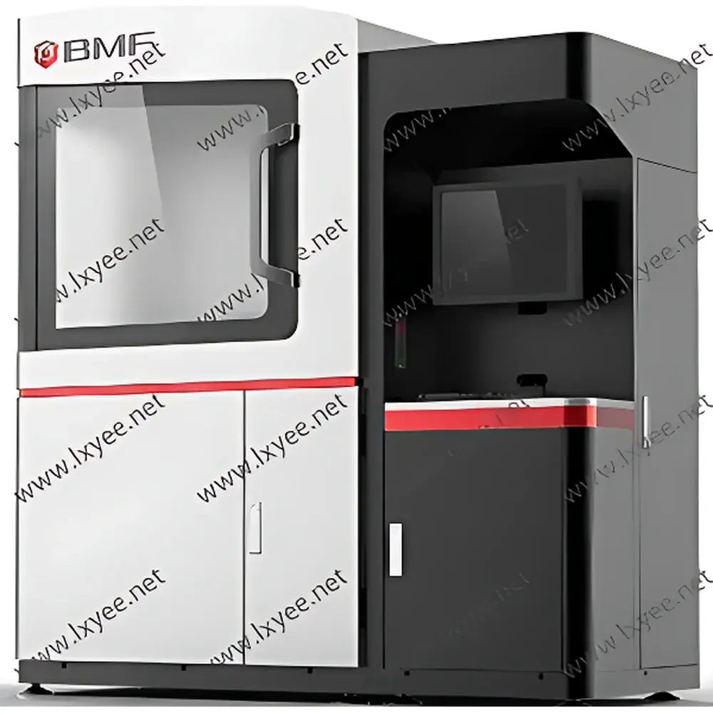
nanoArch P130/S130 Micro-Nano 3D Printer System
| Origin | USA |
|---|---|
| Manufacturer Type | Authorized Distributor |
| Origin Category | Imported |
| Model | P130 / S130 |
| Price Range | USD 280,000 – 420,000 |
| UV Light Source | 405 nm LED |
| XY Resolution | 2–10 µm |
| Layer Thickness | 5–20 µm |
| Build Volume (P130) | 3.84 × 2.16 × 10 mm (Mode 1) / 38.4 × 21.6 × 10 mm (Mode 2) / 50 × 50 × 10 mm (Mode 3) |
| Build Volume (S130) | Up to 100 × 100 × 50 mm |
| Optical System | High-NA Projection Micro-Lithography Optics |
| Post-Processing | Integrated Vacuum Despersion + UV Curing Station |
| Power Requirement | 200–240 V AC, 50/60 Hz, 3 kW |
| Weight | 450 kg |
| Dimensions | 1720 × 650 × 1820 mm |
Overview
The nanoArch P130 and S130 are research-grade micro-nano additive manufacturing systems engineered for high-fidelity fabrication of three-dimensional microstructures with sub-micrometer feature control. Unlike conventional extrusion- or laser-based 3D printing platforms, the nanoArch series employs Projection Micro Litho-Stereolithography Exposure (PμLSE)—a maskless, high-resolution photopolymerization technique derived from semiconductor-grade lithographic principles. In this process, a digitally modulated 405 nm UV-LED light engine projects patterned illumination onto the surface of a photosensitive resin bath via a high-numerical-aperture (NA) optical train. Each exposure layer solidifies a precise 2D cross-section in parallel—enabling rapid, voxel-level control over geometry without mechanical scanning. The system is designed for applications demanding structural fidelity at the 2–10 µm XY resolution range and vertical layer definition down to 5 µm, making it suitable for prototyping photonic crystals, microfluidic manifolds, MEMS scaffolds, metamaterial unit cells, and bio-inspired microarchitectures.
Key Features
- Projection-based micro-stereolithography architecture eliminating point-scanning latency and thermal drift inherent in laser writing systems
- Dual-mode build envelope configuration: P130 supports high-resolution microfabrication (up to 50 × 50 × 10 mm); S130 extends capability to mesoscale parts (up to 100 × 100 × 50 mm) while retaining sub-10 µm lateral resolution
- Integrated air-bearing vibration isolation platform ensuring positional stability during exposure sequences—critical for maintaining registration accuracy across multi-layer stacks
- Real-time optical monitoring subsystem with auto-focus feedback loop compensating for resin meniscus fluctuations and Z-stage thermal expansion
- Modular post-processing station featuring vacuum-assisted resin removal and broadband UV post-cure (365/385/405 nm), compliant with ISO 10993-5 cytotoxicity screening workflows
- Stable 405 nm UV-LED source with <±0.5% intensity drift over 10,000 hours—validated per IEC 62471 photobiological safety standards
Sample Compatibility & Compliance
The nanoArch platform accepts a broad spectrum of commercially available and custom-synthesized photocurable resins—including acrylate-based formulations (e.g., HDDA, PEGDA), ceramic- and metal-nanoparticle-loaded composites, hydrogels for bioprinting, and FDA-listed biocompatible dental and implant-grade monomers. All resin handling protocols conform to ASTM D5237 (photopolymer characterization) and ISO 13485:2016 requirements for medical device manufacturing environments. The system’s mechanical design complies with CE Machinery Directive 2006/42/EC and EMC Directive 2014/30/EU. Optional audit-trail-enabled firmware supports 21 CFR Part 11-compliant electronic records and signatures when deployed in GLP/GMP-regulated laboratories.
Software & Data Management
Control and slicing are executed through proprietary nanoArch Studio software—compatible with Windows 10/11 64-bit and supporting native import of STL, OBJ, and 3MF files. The software implements adaptive mesh refinement, slice-dependent exposure dose mapping, and grayscale lithography algorithms to mitigate stair-stepping artifacts and improve edge acuity. All processing parameters—including exposure time, lift speed, layer offset, and resin-specific attenuation coefficients—are stored in encrypted JSON metadata files. Version-controlled project archives include full calibration logs, stage position histories, and real-time photodiode-integrated exposure monitoring data—enabling full traceability required for ISO/IEC 17025-accredited testing labs.
Applications
- Micro-optics: Fabrication of freeform microlens arrays, diffractive optical elements (DOEs), and integrated waveguide couplers
- Microfluidics: Rapid prototyping of lab-on-chip devices with embedded valves, mixers, and nanochannel networks (down to 500 nm hydraulic diameter)
- Materials science: Additive synthesis of architected metamaterials, lattice structures for compressive strength testing, and gradient-index (GRIN) composites
- Biomedical engineering: Scaffold fabrication for tissue engineering (e.g., osteochondral interfaces), micro-needles, and drug-eluting micro-reservoirs
- Semiconductor R&D: Maskless patterning of sacrificial templates for electroplating, nanoimprint stamp fabrication, and MEMS packaging interposers
FAQ
What lithography principle does the nanoArch system use?
It utilizes Projection Micro Litho-Stereolithography Exposure (PμLSE), a parallel, maskless photopolymerization method based on digital micromirror device (DMD)-driven UV projection.
Is the system compatible with conductive or ceramic-filled resins?
Yes—both P130 and S130 support nanoparticle-doped resins, including silver-, copper-, alumina-, and silica-loaded formulations, provided viscosity remains below 500 mPa·s at 25 °C.
Can the system be integrated into a cleanroom environment?
The nanoArch platform meets ISO Class 5 (Class 100) cleanroom compatibility requirements; optional HEPA-filtered enclosure kits and ESD-safe grounding packages are available.
Does the software support batch processing and remote monitoring?
Yes—via RESTful API integration and scheduled job queues; live status telemetry (exposure count, stage temperature, resin level) is accessible through HTTPS endpoints.
What regulatory documentation is provided for GxP environments?
Factory-issued IQ/OQ protocols, calibration certificates traceable to NIST standards, and 21 CFR Part 11 validation packages are included with enterprise-tier licensing.


