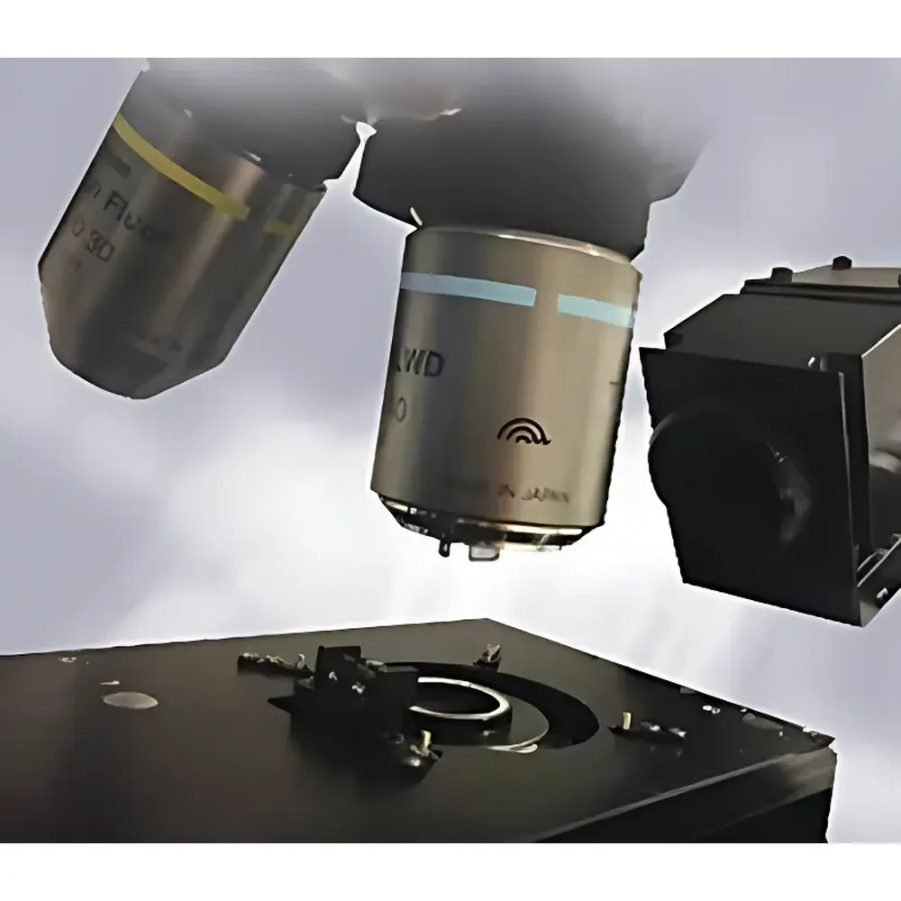
Nanonics MultiView 2500 Infrared Near-Field Scanning Optical Microscope (SNOM) with Integrated Atomic Force Microscopy (AFM)
| Brand | Nanonics |
|---|---|
| Origin | Israel |
| Model | MultiView 2500 |
| Instrument Type | Hybrid SNOM/AFM System |
| Detection Noise (Positional) | 0.2 nm |
| Sample Size Capacity | 6 mm diameter |
| XYZ Scan Range per Stage | >80 µm |
| Dual-Stage Architecture | Probe Stage + Sample Stage |
| Feedback Mechanism | Tuning Fork (TF)-Based AFM |
| Optical Compatibility | Mid-IR to THz spectral range |
| Illumination/Collection Flexibility | Top-, Side-, and Bottom-Optical Access |
Overview
The Nanonics MultiView 2500 is a high-precision, research-grade hybrid near-field scanning optical microscope (SNOM) integrated with atomic force microscopy (AFM), engineered for nanoscale infrared spectroscopic imaging and topographic characterization. Unlike conventional far-field infrared microscopes limited by the diffraction barrier (~λ/2), the MultiView 2500 employs apertureless scattering-type SNOM (s-SNOM) principles—leveraging optical antenna effects at metallic probe tips—to achieve spatial resolution down to ~10–20 nm in the mid-infrared (MIR) regime (2.5–20 µm wavelength). This enables label-free, chemically specific mapping of molecular vibrations (e.g., C=O, C–H, Si–O stretches) with nanoscale fidelity. The system is purpose-built for correlative nanospectroscopy: simultaneous acquisition of topography (via TF-AFM), near-field IR amplitude/phase signals, and far-field reference spectra—essential for materials science, semiconductor metrology, polymer phase analysis, and 2D material heterostructure studies.
Key Features
- Dual independent piezoelectric scanning stages: one dedicated to probe motion, the other to sample translation—each with >80 µm XYZ travel range and sub-0.2 nm closed-loop positional noise floor.
- Tuning fork (TF)-based AFM feedback: eliminates laser interferometric path interference; delivers piconewton (pN)-level force sensitivity in ambient air and liquid environments; compatible with soft biological or polymeric samples.
- Tri-modal optical integration architecture: supports top-illumination (epi-mode), side-illumination (transverse coupling), and bottom-illumination (substrate-coupled) configurations—enabling optimal signal-to-noise ratio across diverse sample geometries and optical properties.
- Modular IR source compatibility: seamlessly interfaces with quantum cascade lasers (QCLs), synchrotron IR beamlines, or broadband thermal sources coupled to Fourier-transform infrared (FTIR) spectrometers.
- Fully programmable LabVIEW-based control suite: provides low-level access to stage motion, lock-in amplifier parameters, laser modulation, and external spectrometer triggering—supporting custom pulse sequences, hyperspectral line scans, and time-resolved near-field dynamics.
Sample Compatibility & Compliance
The MultiView 2500 accommodates standard 6 mm diameter substrates—including Si/SiO₂ wafers, CaF₂ IR windows, gold-coated glass slides, and freestanding graphene membranes—without requiring conductive coating. Its open-stage design permits in situ environmental control (dry N₂ purge, temperature stages up to 300 °C, or electrochemical cells). All mechanical and electronic subsystems conform to CE safety directives (2014/30/EU EMC, 2014/35/EU LVD). Data acquisition workflows support audit-trail generation and user-access logging—facilitating alignment with GLP-compliant laboratories and ISO/IEC 17025 documentation requirements for traceable nanometrology.
Software & Data Management
The native Nanonics Control Software (v6.x) runs on Windows 10/11 with real-time multi-threaded processing. It implements hierarchical data structures compliant with HDF5 format, embedding metadata such as laser wavelength, modulation frequency, demodulation order (n = 1–3), tip enhancement factor calibration, and AFM setpoint parameters. Export modules generate standardized formats (SPE, CSV, TIFF) for third-party analysis in Igor Pro, MATLAB, or Python (SciPy/NumPy). Optional FDA 21 CFR Part 11 compliance packages include electronic signatures, role-based permissions, and immutable raw-data archiving—meeting regulatory expectations for pharmaceutical polymorph characterization or nanomaterial QC reporting.
Applications
- Nanoscale chemical mapping of phase-separated polymer blends (e.g., PS/PVDF) via C–H stretching modes at 2800–3000 cm⁻¹.
- Carrier concentration profiling in doped SiGe heterostructures using free-carrier absorption contrast in the 10–12 µm range.
- Plasmonic hotspot localization in Au nanorod arrays through IR near-field amplitude enhancement at longitudinal resonance.
- In situ degradation monitoring of perovskite solar cell layers under controlled humidity and illumination.
- Correlative topography–conductivity–IR spectroscopy of MoS₂/WSe₂ van der Waals heterojunctions.
FAQ
What infrared spectral ranges are supported by the MultiView 2500?
The system operates across 2.5–20 µm (4000–500 cm⁻¹) using tunable QCLs or broadband thermal sources; extension to THz (30–300 µm) is achievable with appropriate antenna probes and detector integration.
Can the system perform simultaneous topography and IR spectroscopy?
Yes—true simultaneous acquisition is enabled via dual-channel lock-in detection: one channel for AFM topography (tuning fork oscillation amplitude/phase), another for s-SNOM IR signal (scattered field amplitude/phase at nω modulation harmonics).
Is vacuum operation supported?
Standard configuration is ambient air; UHV-compatible versions (≤10⁻⁷ mbar) are available as custom builds with differential pumping stages and ceramic-insulated piezo actuators.
How is tip–sample distance controlled during IR acquisition?
Distance regulation uses the tuning fork’s resonant frequency shift (Δf) as the primary feedback parameter—decoupled from optical detection paths—ensuring stable non-contact operation with <0.5 nm Z-position stability over 1-hour acquisitions.
Does Nanonics provide application-specific probe calibration services?
Yes—certified calibration includes tip apex radius (via SEM/TEM), plasmonic enhancement factor (via reference nanostructures), and IR transmission efficiency (using NIST-traceable Si standards).


