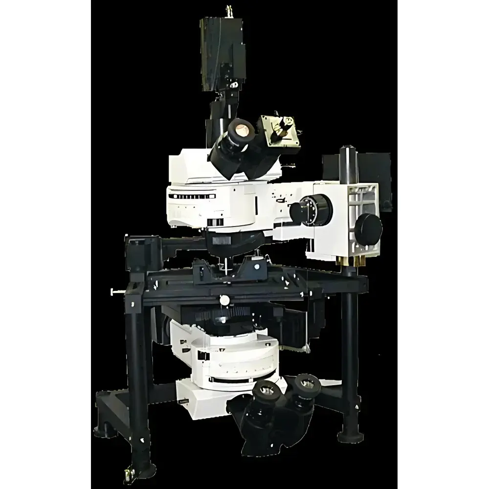
Nanonics MultiView1000 Atomic Force Microscope
| Brand | Nanonics |
|---|---|
| Origin | Israel |
| Model | MultiView1000 |
| Instrument Type | Material-Focused AFM |
| Positional Noise | XY < 20 nm |
| Max Sample Diameter | < 100 mm |
| Max Sample Thickness | < 15 mm |
| Stage Travel Range | 85 µm × 85 µm |
Overview
The Nanonics MultiView1000 Atomic Force Microscope (AFM) is a high-precision, multi-modal scanning probe microscopy platform engineered for nanoscale topographic, mechanical, optical, and functional characterization of materials across research and industrial laboratories. Unlike conventional single-mode SPM systems, the MultiView1000 integrates atomic force microscopy with near-field scanning optical microscopy (NSOM), enabling simultaneous or sequential acquisition of topography, nanomechanical properties (e.g., elasticity, adhesion), local optical response (fluorescence, photoluminescence, Raman coupling), and electro-thermal signals — all within a single, co-registered coordinate frame. Its core architecture leverages piezoelectric tube scanners with sub-nanometer closed-loop positioning stability and low-drift thermal design, optimized for operation in ambient, liquid, vacuum, and cryogenic environments (down to 4 K). The system is purpose-built for correlative multimodal analysis where spatial registration fidelity between physical and optical contrast mechanisms is critical — such as in semiconductor defect metrology, soft biomaterials imaging under physiological conditions, or plasmonic nanostructure characterization.
Key Features
- True hybrid AFM-NSOM platform supporting concurrent or sequential topographic, optical, and functional imaging
- Flexible scanning configuration: tip-scanning or sample-scanning modes compatible with contact, tapping (AC), and non-contact AFM operation
- Low-noise positioning performance: XY positional noise < 20 nm; Z noise < 0.3 nm (RMS, bandwidth-dependent)
- Modular scanner options: standard 85 µm × 85 µm travel range; optional 30 µm and 10 µm high-resolution scanners with sub-0.1 nm step resolution
- Universal probe compatibility: supports commercial NSOM probes, conductive AFM tips, hollow cantilevers, insulated glass nanowires, dual-wire configurations, and micro-pipettes for localized fluid/gas delivery and in situ reaction studies
- Integrated environmental control: fully compatible with cryostats (liquid helium), ultra-high vacuum chambers, and sealed reaction cells with automated gas/liquid injection
- Optical integration-ready: designed for seamless coupling with confocal microscopes, micro-Raman spectrometers, SEM columns, and SHG/THG platforms
Sample Compatibility & Compliance
The MultiView1000 accommodates samples up to 100 mm in diameter and 15 mm in thickness, with programmable stage alignment for off-center or irregular substrates. Its open-access design allows direct integration into cleanroom workflows and glovebox environments. All hardware and software components comply with international safety standards including IEC 61010-1 (electrical safety) and ISO 14001-aligned environmental design principles. Data acquisition protocols support audit-trail generation and user access control in accordance with GLP and GMP requirements. While not FDA-cleared as a medical device, the system meets ASTM E2539–22 guidelines for SPM performance verification and is routinely deployed in ISO/IEC 17025-accredited laboratories for nanomaterial certification.
Software & Data Management
The MultiView1000 operates via Nanonics’ proprietary NT software suite, compatible with Windows 10/11 (64-bit) and offering real-time multi-channel image acquisition (up to 8 synchronized inputs), advanced 3D surface reconstruction, cross-sectional profiling, and quantitative nanomechanical mapping (e.g., modulus, dissipation, adhesion histograms). LabVIEW-based drivers enable custom automation and integration with third-party DAQ systems (NI PXI, Keysight). All acquired data are stored in vendor-neutral HDF5 format with embedded metadata (scan parameters, calibration constants, timestamp, user ID), ensuring long-term reproducibility and FAIR (Findable, Accessible, Interoperable, Reusable) compliance. Software modules include automated tip qualification, drift correction algorithms, and batch processing pipelines for statistical surface analysis per ISO 25178.
Applications
- Materials Science: Quantitative roughness analysis (Sa, Sq), grain boundary mapping, nanomechanical property gradients in composites, wear track quantification, and thin-film island distribution
- Life Sciences: Live-cell membrane dynamics in buffer solution, pore formation kinetics, cytoskeletal stiffness mapping, and ligand-receptor interaction forces under physiological conditions
- Semiconductor Metrology: Critical dimension (CD) verification of FinFET structures, dopant profiling via Kelvin probe force microscopy (KPFM), and gate oxide defect localization
- Data Storage: Magnetic domain imaging on HDD media, read/write head wear analysis, and nanoscale friction coefficient mapping
- Nano-Optics & Plasmonics: Sub-diffraction-limit fluorescence mapping of quantum dots, photoluminescence hot-spot correlation with topography, and plasmonic mode excitation via NSOM-PL
- Failing Analysis: Electrical leakage path identification, interconnect delamination assessment, and bond pad interface integrity evaluation using conductive-AFM and scanning capacitance microscopy (SCM)
FAQ
Is the MultiView1000 compatible with third-party SPM controllers or software?
Yes — Nanonics provides open API documentation and LabVIEW/VISA drivers for integration with external control systems and custom analysis pipelines.
Can NSOM and AFM measurements be acquired simultaneously?
Yes — the system supports true concurrent acquisition using separate optical and mechanical detection paths, preserving spatial registration at the nanometer level.
What environmental conditions can the system operate under?
The platform supports ambient air, controlled humidity, liquid immersion, ultra-high vacuum (<10⁻⁹ mbar), and cryogenic temperatures down to 4 K using integrated cryostat interfaces.
Does the system meet regulatory requirements for quality-controlled labs?
It supports 21 CFR Part 11-compliant electronic signatures and audit trails when configured with validated software modules and documented calibration procedures.
Are custom scanner or probe holder configurations available?
Yes — Nanonics offers application-specific mechanical redesign services, including large-area scanners (up to 200 µm), inverted optical access mounts, and MEMS-integrated probe carriers.


