Nanonics MV1000/MV2000/MV4000 Scanning Electrochemical Microscope (SECM) Integrated with Atomic Force Microscopy
| Brand | Nanonics |
|---|---|
| Model | MV1000 / MV2000 / MV4000 |
| Instrument Type | AFM-Integrated Scanning Electrochemical Microscope |
| Z-Positioning Noise | 0.2 nm |
| Sample Diameter | < 6 mm |
| XYZ Scan Range | 80 µm × 80 µm × 80 µm |
| Probe | Hollow glass nanopipette with Pt nanowire electrode (50–100 nm tip diameter) |
| Electrochemical Control | Bipotentiostat (±10 V, ±0.25 A), current sensitivity: 10⁻¹²–0.1 A/V |
| Compatible Electrodes | Up to four side-mounted or back-contacted reference/counter electrodes (e.g., Ag/AgCl) |
| Liquid Cell Material | PEEK |
| Optical Access | Fully open top and bottom optical pathways |
| Environmental Options | Optional inert-gas chamber (N₂/Ar) |
| Software Compliance | Supports audit trail, user access control, and data integrity per FDA 21 CFR Part 11 requirements |
Overview
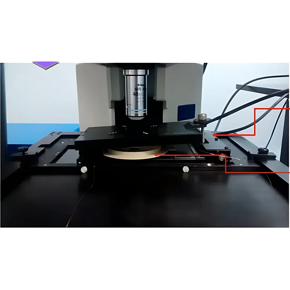
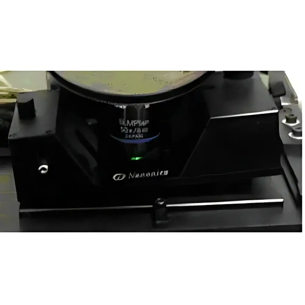
The Nanonics MV1000/MV2000/MV4000 Scanning Electrochemical Microscope (SECM) is a fully integrated hybrid platform combining high-resolution atomic force microscopy (AFM) with quantitative electrochemical imaging and spectroscopic correlative capabilities. Engineered for precision nanoscale electrochemical characterization, the system operates on the principle of feedback-mode SECM—where local faradaic current generated by redox mediator regeneration at an ultramicroelectrode (UME) tip is measured as a function of tip–sample distance. Unlike conventional SECM systems, Nanonics’ architecture embeds real-time AFM topographic feedback directly into the electrochemical scanning loop, enabling stable, collision-free operation even on highly sloped or heterogeneous surfaces. This co-registered AFM-SECM capability ensures simultaneous acquisition of nanomechanical, topographic, and electrochemical activity maps with sub-100 nm spatial resolution and sub-picoampere current sensitivity. The system is designed for operation in ambient, liquid, or controlled inert-gas environments, supporting both static and dynamic electrochemical processes—including in situ electrocatalysis, corrosion studies, battery interface analysis, and bioelectrochemical mapping.
Key Features
- AFM-guided SECM feedback control: Eliminates tip crash risk during electrochemical scanning by dynamically maintaining constant tip–sample separation via piezoelectric Z-feedback.
- Patented cantilever-mounted hollow glass nanopipette probes: Feature Pt nanowire electrodes (50–100 nm diameter), enabling high spatial resolution and unobstructed vertical optical access for simultaneous optical microscopy or Raman coupling.
- Modular bipotentiostat integration: Delivers ±10 V potential range and ±0.25 A current compliance, with programmable current sensitivity from 10⁻¹² A/V to 0.1 A/V—optimized for both low-current biosensing and high-current electrocatalytic measurements.
- Dual scanning modes: Supports both sample-scanning and probe-scanning configurations across 80 µm × 80 µm × 80 µm XYZ ranges, accommodating diverse sample geometries and experimental constraints.
- PEEK-based electrochemical liquid cell: Chemically resistant, electrically insulating, and compatible with aqueous and organic electrolytes; includes provision for up to four side-mounted reference/counter electrodes and optional back-contact wiring.
- Open-top/bottom optical architecture: Enables full compatibility with inverted microscopes, confocal systems, micro-Raman spectrometers, and nonlinear optical techniques such as SHG or TERS.
- Expandable environmental control: Optional gas-tight chamber supports N₂ or Ar purging for oxygen-sensitive experiments, including Li-ion battery SEI formation or enzymatic redox studies.
Sample Compatibility & Compliance
The Nanonics SECM platform accommodates samples up to 6 mm in diameter and up to 10 mm in height (with appropriate stage adapters). It supports conductive, semiconductive, and insulating substrates—including ITO-coated glass, Si wafers, carbon electrodes, biological membranes, and polymer electrolytes. All liquid cells meet ISO 17025-relevant design criteria for reproducible electrochemical cell geometry and minimized uncompensated resistance. The system complies with GLP and GMP documentation standards through its software’s electronic signature support, audit trail logging, and role-based user permissions—fully aligned with FDA 21 CFR Part 11 requirements for regulated laboratories. Electrical safety conforms to IEC 61010-1; electromagnetic compatibility meets EN 61326-1.
Software & Data Management
Nanonics’ proprietary NanoNavigator™ software provides unified control of AFM, SECM, and optional spectroscopic modules within a single GUI. It supports automated calibration routines for probe resistance, tip–sample capacitance, and Faradaic current baseline correction. Real-time data streams—including topography, current, dI/dZ, and phase—are stored in vendor-neutral HDF5 format with embedded metadata (timestamp, instrument configuration, operator ID, environmental conditions). Batch processing tools enable quantitative current mapping, approach curve fitting (using Fickian diffusion models), and statistical analysis of electrochemical heterogeneity. Export options include CSV, MATLAB (.mat), and ImageJ-compatible TIFF stacks. Software validation packages—including IQ/OQ documentation templates and traceable calibration protocols—are available for regulated QA/QC environments.
Applications
- Electrocatalyst screening: Mapping local activity of Pt/C, NiFe LDH, or single-atom catalysts under operando conditions.
- Battery interface science: Imaging solid-electrolyte interphase (SEI) growth kinetics and ion transport barriers on anode/cathode surfaces.
- Corrosion science: Resolving localized pitting initiation sites and passivation layer breakdown potentials on stainless steel or Al alloys.
- Biointerface studies: Quantifying electron transfer rates across immobilized enzymes, redox proteins, or microbial biofilms.
- Microfabricated device testing: Characterizing leakage currents, edge effects, and electrochemical uniformity in MEMS sensors or lab-on-chip electrodes.
- Correlative multimodal imaging: Simultaneous AFM-SECM-Raman mapping of stress-induced electrochemical activity in 2D materials (e.g., MoS₂ edge reactivity).
FAQ
What distinguishes Nanonics’ SECM from conventional standalone SECM systems?
Nanonics integrates real-time AFM topographic feedback directly into the electrochemical scanning algorithm—preventing tip–sample collisions and enabling reliable operation on rough or tilted surfaces without manual Z-height adjustment.
Can the system operate in air, liquid, and inert atmosphere simultaneously?
No—environmental mode must be selected per experiment. However, the platform supports rapid reconfiguration between ambient, liquid-cell, and inert-gas chamber setups using standardized mechanical interfaces.
Is third-party probe compatibility supported?
Yes. The system accepts standard SPM probe holders and is mechanically and electrically compatible with commercial conductive AFM probes, though Nanonics’ patented glass nanopipettes are required for full SECM functionality.
Does the software support automated data analysis for SECM approach curves?
Yes. NanoNavigator includes built-in fitting modules for theoretical SECM approach curve models (e.g., hemispherical diffusion, substrate generation/tip collection), with parameter extraction for tip radius, diffusion coefficient, and kinetic rate constants.
What level of training and application support is provided?
Nanonics offers on-site installation, operator certification, and application-specific method development workshops—delivered by field application scientists with PhD-level expertise in electrochemistry and SPM instrumentation.


