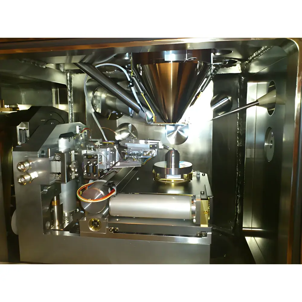
Nanonics MV4000 AFM-SEM-Raman Correlative Microscopy System
| Brand | Nanonics |
|---|---|
| Origin | Israel |
| Model | MV4000 |
| Instrument Type | Material-Focused Hybrid Correlative Microscope |
| Positional Detection Noise | 0.2 nm |
| Maximum Sample Diameter | <100 mm |
| Maximum Sample Thickness | <15 mm |
| Sample Stage Travel Range | 85 × 85 × 85 µm |
Overview
The Nanonics MV4000 is a fully integrated, multi-modal correlative microscopy platform engineered for nanoscale structural, mechanical, electrical, optical, and chemical characterization. Unlike conventional standalone instruments, the MV4000 enables true concurrent or sequential operation of Atomic Force Microscopy (AFM), Scanning Electron Microscopy (SEM), and Confocal Raman Spectroscopy — all within a single vacuum-compatible sample chamber or under controlled environmental conditions. Its core architecture leverages Nanonics’ proprietary probe-integrated SEM/FIB-compatible stage design, permitting real-time, beam-synchronized SPM measurements during electron or ion beam irradiation. This capability is grounded in precision piezoelectric positioning, low-noise interferometric displacement sensing (<0.2 nm RMS positional detection noise), and optomechanically decoupled probe actuation — ensuring high-fidelity topographic, nanomechanical, and spectroscopic data acquisition without cross-modality interference.
Key Features
- True hybrid correlative operation: Simultaneous or time-synchronized AFM + SEM + Raman imaging and spectroscopy on identical sample regions
- SEM/FIB-compatible SPM stage with full probe visibility under electron beam — enabling direct tip navigation, in situ tip alignment, and real-time beam–probe interaction monitoring
- Open-architecture NanoToolKit probe interface: Supports functionalized cantilevers (conductive, thermal, optical, magnetic, electrochemical) with standardized electrical and optical feedthroughs
- Vacuum-compatible sample chamber (optional UHV configuration) with integrated heating/cooling stages and electrical biasing capabilities (±10 V, 100 MHz bandwidth)
- Sub-nanometer spatial registration accuracy between modalities via shared coordinate referencing and drift-compensated stage control
- Modular Raman integration: 532 nm or 785 nm excitation lasers, spectral resolution ≤2 cm⁻¹, CCD or EMCCD detection, confocal pinhole adjustable from 25–200 µm
Sample Compatibility & Compliance
The MV4000 accommodates solid, conductive or insulating samples up to 100 mm in diameter and 15 mm in thickness — compatible with standard SEM stubs, TEM grids, MEMS wafers, and packaged semiconductor devices. Its stage design complies with ISO 14644-1 Class 5 cleanroom handling protocols and supports GLP-compliant sample loading workflows. All electronic subsystems meet CE/IEC 61000-6-3 EMC emission standards and IEC 61010-1 safety requirements for laboratory instrumentation. Data acquisition firmware supports audit-trail logging per FDA 21 CFR Part 11 guidelines when configured with user authentication and electronic signature modules.
Software & Data Management
Control and correlation are managed through Nanonics’ CorrelateSuite™ software — a modular, Python-extendable platform supporting synchronized acquisition, multi-dimensional data fusion (e.g., AFM topography + SEM secondary electron contrast + Raman chemical maps), and quantitative overlay analysis. The software includes native support for ASTM E2932 (Standard Guide for Correlative Microscopy), ISO/IEC 17025 traceability metadata embedding, and export formats compliant with HDF5, TIFF stack, and NIST-recommended spectral interchange (JCAMP-DX). Raw data archives include full instrument configuration logs, environmental sensor records (temperature, pressure, vibration), and probe calibration history — essential for regulatory review and inter-laboratory reproducibility validation.
Applications
- Nanoscale failure analysis in advanced packaging: Localized strain mapping (AFM) overlaid with defect morphology (SEM) and interfacial chemistry (Raman) at solder joints or TSV interfaces
- In situ radiation damage studies: Real-time AFM nanomechanical response during focused ion beam (FIB) milling or electron irradiation
- 2D material heterostructure characterization: Layer-dependent modulus (AFM), edge contrast (SEM), and phonon mode shifts (Raman) correlated at sub-100 nm resolution
- Photonic device metrology: Near-field optical coupling (via SNOM-capable probes) combined with SEM-guided placement and Raman-based carrier concentration profiling
- Defense-grade thin-film sensor development: Multi-parameter testing under thermal cycling, including piezoresistive response (AFM), surface degradation (SEM), and bond stability (Raman)
FAQ
Can the MV4000 operate all three modalities simultaneously?
Yes — AFM force feedback, SEM imaging, and Raman spectral acquisition can be synchronized using shared trigger logic and time-stamped data streams. Beam blanking and laser gating ensure no signal crosstalk.
Is the system compatible with existing SEM/FIB platforms?
The MV4000 is available as a retrofit module for selected Thermo Fisher, Zeiss, and JEOL SEM/FIB systems, with custom flange adapters and vacuum interface certification provided.
What level of spatial correlation accuracy is achievable between modalities?
Typical registration uncertainty is ≤50 nm across the central 50 × 50 µm field-of-view, verified using NIST-traceable grating standards and iterative image-based registration algorithms.
Does the system support automated tip exchange inside the chamber?
No — tip exchange requires atmospheric break; however, the NanoToolKit interface allows rapid (<5 min) in-chamber probe swapping with pre-aligned calibration routines.
Are there application-specific compliance packages available?
Yes — optional GMP-ready configurations include IQ/OQ documentation, calibration certificates traceable to NIST standards, and 21 CFR Part 11-compliant software validation kits for pharmaceutical or medical device QA/QC labs.


