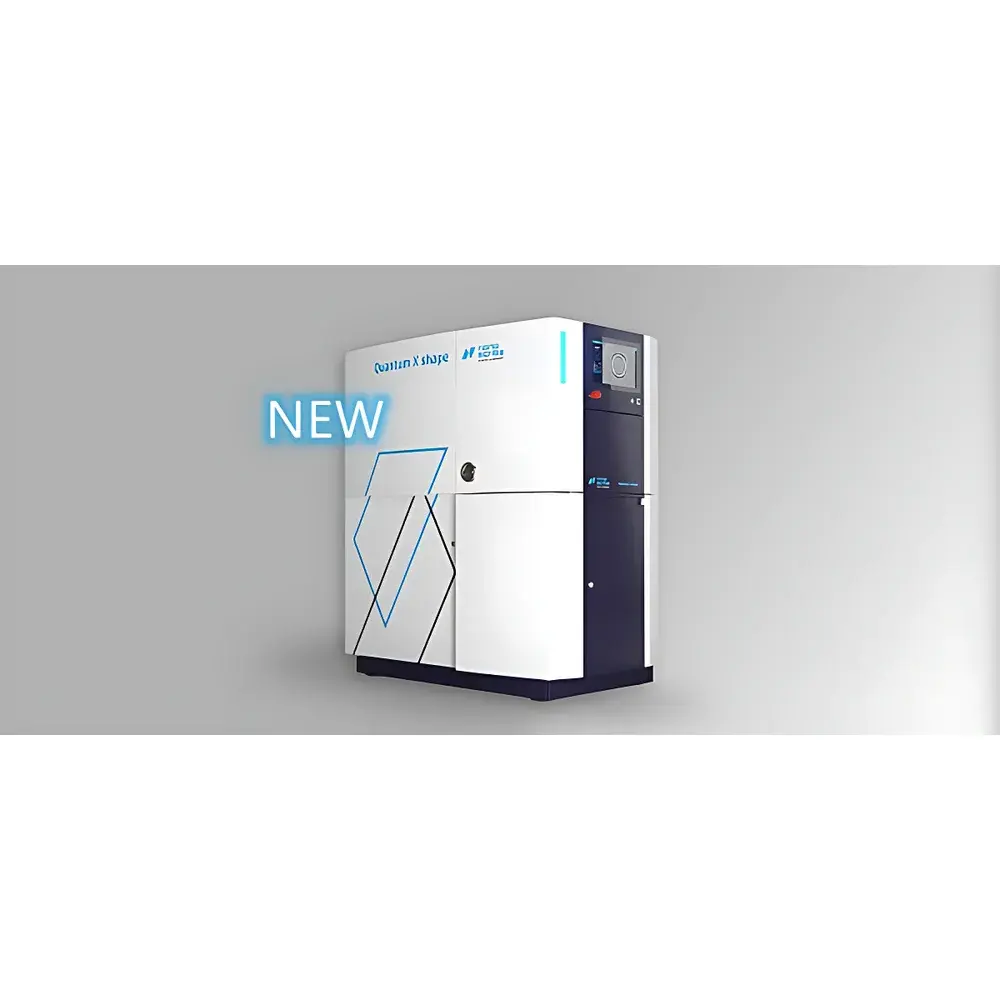
Nanoscribe Quantum X shape Two-Photon Direct Laser Writing System
| Brand | Nanoscribe |
|---|---|
| Origin | Germany |
| Manufacturer Type | Authorized Distributor |
| Product Origin | Imported |
| Model | Quantum X shape |
| Price Range | USD 650,000 – 1,050,000 (FOB Hamburg) |
| Maximum Build Area | 152 mm (6-inch wafer compatible) |
| Layer Resolution (Z) | 0.3–5 µm |
| Laser Source | Femtosecond Ti:Sapphire Oscillator, 250 mW average power @ 780 nm |
| Feature Size Resolution | ≤200 nm (lateral), down to 100 nm with optimized parameters and materials |
| Surface Roughness (Ra) | <5 nm |
| Maximum Scanning Speed | 6.25 m/s (at 2× objective magnification) |
| Compatible Materials | Photopolymerizable resins (including IP-series, OrmoComp®, SZ2080, hybrid organic-inorganic formulations) |
Overview
The Nanoscribe Quantum X shape is a two-photon direct laser writing (TPDLW) system engineered for sub-100 nm resolution 3D micro- and nanofabrication. Unlike conventional stereolithography (SLA) or digital light processing (DLP) systems, it employs nonlinear two-photon absorption within photosensitive resins—enabling true volumetric voxel-by-voxel fabrication with diffraction-unlimited spatial confinement. This principle permits arbitrary 3D geometry definition—including high-aspect-ratio microstructures, freeform optical elements, and monolithic microfluidic networks—without masks, molds, or layer-by-layer planar constraints. Designed for both R&D prototyping and wafer-scale production, the Quantum X shape bridges the gap between academic nanofabrication and industrial-grade process repeatability. Its architecture integrates high-stability optical path alignment, active thermal management, and vacuum-compatible sample stages—ensuring long-term dimensional stability across multi-hour exposure sequences.
Key Features
- Sub-100 nm feature resolution enabled by adaptive voxel modulation and a 100 nm computational processing grid
- High-speed galvo-scanning optics delivering up to 6.25 m/s scan velocity while maintaining trajectory fidelity via real-time beam position feedback
- Automated self-calibration routines for laser energy homogeneity, focus drift compensation, and stage positioning accuracy
- Integrated touch interface for on-system job setup, live status monitoring, and parameter validation prior to exposure
- Wafer-scale compatibility: supports 100 mm (4″), 150 mm (6″), and custom substrates up to Ø152 mm with flatness tolerance <1 µm
- Overnight throughput of ≥200 standardized mesoscale features (e.g., micro-lenses, photonic crystals, or micro-pillar arrays) under unattended operation
- Modular material compatibility: validated with Nanoscribe IP-Dip, IP-L, IP-S, OrmoComp®, SZ2080, and third-party acrylate/epoxy-based resins
- Optimized for both single-shot prototyping and batch-mode production workflows, including alignment to pre-patterned wafers and fiducial-based stitching
Sample Compatibility & Compliance
The Quantum X shape accommodates rigid and semi-rigid substrates including silicon wafers, fused silica, sapphire, ITO-coated glass, and polymer films (e.g., PET, PI). Sample mounting utilizes vacuum chucks and kinematic alignment pins for repeatable registration. The system complies with CE marking requirements (2014/30/EU EMC Directive, 2014/35/EU LVD Directive) and conforms to ISO 14644-1 Class 5 cleanroom operational guidelines when installed in controlled environments. All optical components meet ISO 10110 surface quality standards; laser safety classification is EN 60825-1:2014 Class 4. Process documentation supports GLP/GMP traceability when paired with oConnectX audit logging (21 CFR Part 11-compliant electronic signatures optional).
Software & Data Management
oConnectX software serves as the unified control, simulation, and data management platform. It includes mesh-to-voxel conversion with adaptive slicing, dose optimization algorithms based on material absorption coefficients, and real-time exposure dose mapping. Project files are stored in encrypted SQLite databases with immutable version history and user-specific access permissions. Remote monitoring is supported via TLS-secured WebSocket connections, enabling multi-site collaboration and centralized fleet management. Export formats include STL (with sub-micron tessellation), G-code (for hybrid lithography workflows), and HDF5 (for quantitative metrology integration with AFM or SEM datasets). Audit trails record operator actions, parameter changes, environmental logs (temperature/humidity), and laser power calibration events.
Applications
The Quantum X shape enables functional device fabrication across multiple disciplines: micro-optics (gradient-index lenses, metasurfaces, waveguides), biomedical scaffolds (vascular mimetics, neural probes), MEMS actuators and sensors, microfluidic mixers and droplet generators, photonic crystals, mechanical metamaterials, and anti-reflective or superhydrophobic surface textures. Its ability to write directly onto processed wafers makes it suitable for post-CMOS integration of photonic interposers or micro-opto-electro-mechanical systems (MOEMS). In academic settings, it supports rapid iteration of design-of-experiments (DoE) for material-process interaction studies; in industry, it facilitates pilot-line qualification of microstructured components compliant with ASTM F2792 (additive manufacturing terminology) and ISO/ASTM 52900 standards.
FAQ
What is the minimum printable feature size achievable with standard process parameters?
Under optimized conditions using IP-Dip resin and a 63× oil-immersion objective, lateral features ≤100 nm and axial features ≤200 nm are routinely achieved.
Is the system compatible with cleanroom Class 100 (ISO 5) environments?
Yes—the base unit meets vibration and outgassing specifications for ISO 5 installation; optional HEPA-filtered enclosure kits are available.
Can the Quantum X shape perform grayscale lithography?
Yes—it natively supports two-photon grayscale lithography (2GL®), enabling continuous topography modulation with <5 nm vertical step resolution.
Does Nanoscribe provide material certification data for biocompatibility or USP Class VI compliance?
Material-specific biocompatibility reports (ISO 10993-5 cytotoxicity, USP <87>) are available upon request for IP-L and IP-S resins.
How is system calibration maintained over extended operation?
Automated daily calibration sequences verify galvo linearity, focus stability, and laser power uniformity; all results are archived in the oConnectX audit log.


