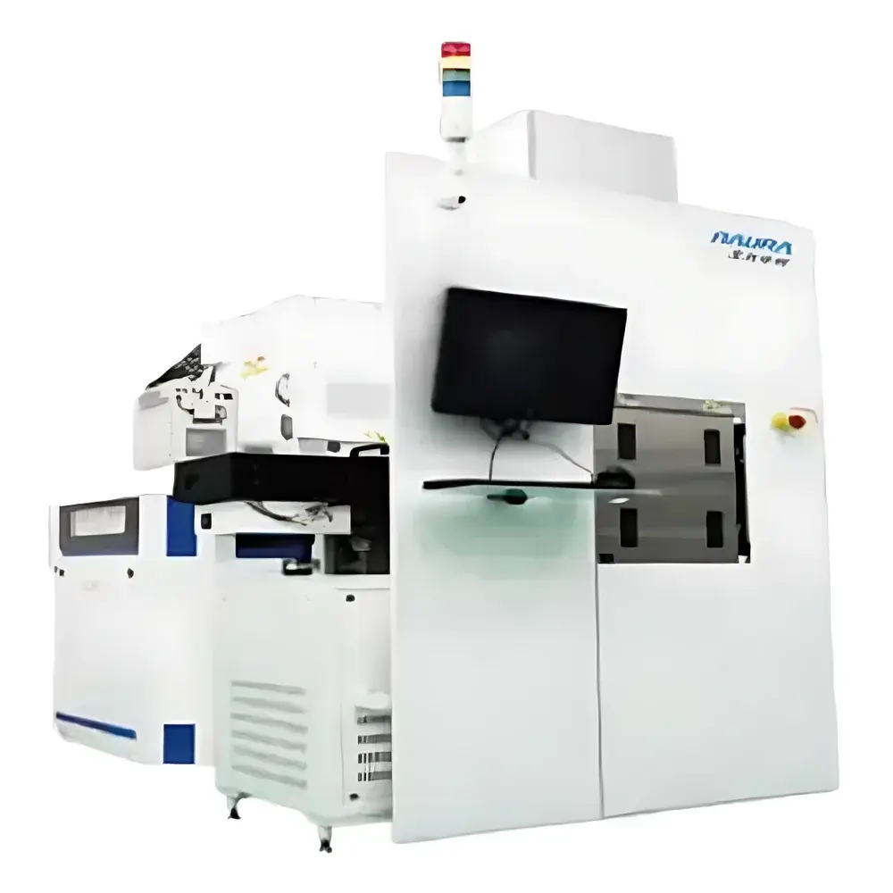
NAURA GSE C200 Multi-Function Plasma Etching System
| Brand | NAURA |
|---|---|
| Origin | Beijing, China |
| Model | GSE C200 |
| Wafer Size Capacity | ≤8-inch |
| Plasma Source Type | High-Density Inductively Coupled Plasma (ICP) |
| Etch Uniformity | <±3% (1σ, across 200 mm wafer) |
| Material Compatibility | Si, SiO₂, Si₃N₄, GaN, GaAs, InP, LiNbO₃, Nb, PI, metals, organics |
| Application Scope | R&D, failure analysis, pilot-line process development |
| Compliance | Designed to meet SEMI S2/S8 safety guidelines |
| Software | Integrated recipe management with audit trail logging (21 CFR Part 11–ready configuration available) |
Overview
The NAURA GSE C200 Multi-Function Plasma Etching System is an advanced inductively coupled plasma (ICP) etcher engineered for high-precision, low-damage material removal in semiconductor research, process development, and small-batch production environments. Leveraging a high-density ICP source with independent RF bias control, the system delivers stable plasma generation across a wide range of process gases—including CF₄, CHF₃, Cl₂, BCl₃, SF₆, O₂, and Ar—enabling both isotropic and anisotropic etching profiles. Its chamber architecture supports uniform power coupling and optimized radical/ion flux distribution, resulting in repeatable etch rates and sub-3% within-wafer uniformity (1σ) on 200 mm substrates. The GSE C200 is not a production-line cluster tool but a standalone, modular platform designed for rapid process transfer from lab to fab—validated in multiple domestic IC front-end fabs and compound semiconductor pilot lines handling GaN-on-Si, RF filters, photonic integrated circuits (PICs), and MEMS devices.
Key Features
- Modular high-density ICP source with adjustable coil geometry and impedance-matching network for fine-tuned plasma density control (1×10¹¹–5×10¹¹ cm⁻³ typical)
- Dual-frequency RF delivery: 13.56 MHz ICP source + 2 MHz/400 kHz bias RF for independent ion energy and flux regulation
- Temperature-controlled electrostatic chuck (ESC) with helium backside cooling (±0.5 °C stability) for thermal management during high-power etching
- Quartz-shielded process chamber with corrosion-resistant anodized aluminum walls and automated pressure control (1–100 mTorr range)
- Integrated real-time endpoint detection via optical emission spectroscopy (OES) with configurable wavelength bands (200–800 nm)
- Tool-to-tool recipe portability supported by standardized XML-based process file structure compliant with SECS/GEM interface protocols
Sample Compatibility & Compliance
The GSE C200 accommodates wafers up to 200 mm (8-inch) diameter, including standard silicon, SOI, quartz, sapphire, and flexible polymer substrates. It demonstrates robust performance on dielectric layers (SiO₂, Si₃N₄, Al₂O₃), compound semiconductors (GaN, GaAs, InP, GaSb), ferroelectric materials (LiNbO₃), refractory metals (Nb, Ti, Mo), and polymeric films (PI, BCB, PMMA). All wet-clean-compatible hardware surfaces meet SEMI F22 surface finish specifications. The system is built to comply with SEMI S2 (safety) and S8 (ergonomics) standards; optional configurations include full GLP/GMP audit trail logging, electronic signature support per FDA 21 CFR Part 11, and integration-ready Modbus TCP and SECS/GEM communication stacks for factory automation.
Software & Data Management
The NAURA ETCHware™ control suite provides intuitive graphical interface for recipe creation, parameter monitoring, and fault diagnostics. Each run generates timestamped log files containing chamber pressure, RF forward/reflected power, gas flow rates, ESC temperature, and OES intensity traces. Historical data is stored in SQLite format with SHA-256 checksum validation. For regulated environments, optional 21 CFR Part 11 mode enables role-based user access, electronic signatures, and immutable audit trails with operator ID, action type, and time stamp. Raw sensor data can be exported in CSV or HDF5 format for offline statistical process control (SPC) analysis using JMP, Python pandas, or MATLAB.
Applications
The GSE C200 serves as a primary etch platform in university cleanrooms, national laboratories, and corporate R&D centers developing next-generation devices. Typical use cases include: defining high-aspect-ratio trenches in Si for MEMS accelerometers; patterning GaN HEMT gate recesses with sub-5 nm CD control; removing residual photoresist after lift-off without substrate damage; selective etching of AlGaN barriers in UV LED structures; and cross-sectional sample preparation for TEM/FIB analysis. Its flexibility extends to failure analysis labs performing localized defect isolation via focused plasma etching, and to photonics groups fabricating grating couplers in SiN waveguides.
FAQ
What wafer sizes does the GSE C200 support?
The system is configured for 100 mm, 150 mm, and 200 mm wafers; manual loading is supported for non-standard substrates such as diced dies or rectangular samples up to 210 mm diagonal.
Is remote monitoring and control available?
Yes—standard Ethernet connectivity supports VNC-based remote desktop access and optional OPC UA server integration for MES-level data exchange.
Can the GSE C200 be upgraded to support 300 mm wafers?
No—the mechanical and vacuum architecture is optimized for ≤200 mm platforms; NAURA offers the GSE C300 series for 300 mm applications.
Does the system include process qualification documentation?
Each shipment includes IQ/OQ documentation templates aligned with ISO/IEC 17025 requirements; full PQ support is provided upon request for GMP-regulated facilities.
What maintenance intervals are recommended?
Chamber cleaning every 50–100 runs depending on process chemistry; RF matching network calibration quarterly; OES window replacement annually under normal usage conditions.


