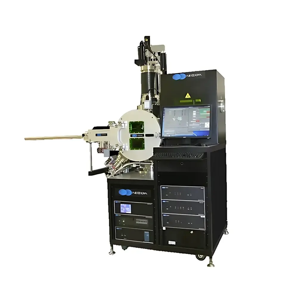
Neocera Large-Area PLD System for Epitaxial Thin Film Deposition
| Brand | Neocera |
|---|---|
| Origin | USA |
| Model | Large-Area PLD Systems |
| Substrate Diameter | 4" (100 mm), 6" (150 mm), 8" (200 mm) |
| Chamber Type | 18-inch-diameter spherical or cylindrical vacuum chamber |
| Max. Substrate Temperature | 850 °C (for 4″), 750 °C (for 6″), 700 °C (for 8″) |
| Target Mount | 4 × 2-inch rotary target assembly |
| Thickness Uniformity | ±5% or better across full wafer |
| Process Gases | O₂, N₂, Ar with mass flow controllers (MFCs) |
| Load Lock | Integrated |
| Automation Platform | Windows 7 + LabVIEW 2013 |
| Laser Scanning | Programmable beam rastering with inverse-velocity dwell-time compensation |
| Oxygen-Compatible High-Temperature Operation | Yes |
Overview
The Neocera Large-Area Pulsed Laser Deposition (PLD) System is an engineered solution for high-precision, scalable epitaxial thin film synthesis on semiconductor-grade wafers up to 200 mm (8 inch) in diameter. Operating on the fundamental principle of pulsed laser ablation in controlled reactive atmospheres, this system enables stoichiometric transfer of complex multi-element oxides, nitrides, and chalcogenides from solid targets onto heated substrates under ultra-high vacuum (UHV) or low-pressure process gas environments. Unlike sputtering or CVD techniques, PLD preserves target stoichiometry during ablation—critical for functional oxides such as YBCO, LSMO, PZT, and STO where cation ratios directly govern electronic, ferroelectric, or superconducting behavior. The system’s large-area capability bridges the gap between research-scale deposition and pilot-line compatibility, supporting both R&D prototyping and pre-production material qualification in accordance with semiconductor industry dimensional and thermal specifications.
Key Features
- Full-wafer deposition support for 100 mm (4″), 150 mm (6″), and 200 mm (8″) substrates with integrated rotation and programmable laser scanning
- Neocera-patented laser beam rastering mechanism that maintains constant fluence (J/cm²) across the target surface via inverse-velocity dwell-time control—ensuring reproducible ablation plume density and film thickness linearity
- Oxygen-compatible high-temperature substrate heating: up to 850 °C for 4″ wafers, 750 °C for 6″, and 700 °C for 8″—enabling thermodynamically stable growth of metal oxides under oxidizing conditions
- Modular 18-inch-diameter spherical or cylindrical UHV chamber architecture with all-metal sealing, bake-out capability, and base pressure <5×10⁻⁸ Torr
- Four-position 2-inch-diameter rotating target holder for sequential or combinatorial deposition of multilayer heterostructures and superlattices
- Integrated load lock with automated gate valve operation for rapid sample exchange without breaking main chamber vacuum
- Mass flow-controlled reactive gas delivery (O₂, N₂, Ar) with digital MFCs calibrated per ASTM E2653–19 standards for process repeatability
Sample Compatibility & Compliance
This PLD platform accommodates rigid, flat substrates including Si, SrTiO₃, MgO, LaAlO₃, Al₂O₃ (sapphire), and flexible metallic foils (e.g., Ni-based tapes) when mounted on compatible carriers. It supports epitaxial growth of single-crystal films with orientation control verified by in-situ or ex-situ XRD and RHEED. The system conforms to ISO 14644-1 Class 5 cleanroom integration requirements and meets mechanical safety standards per ANSI/UL 61010-1. All vacuum components comply with ASME BPVC Section VIII Div. 1 pressure vessel regulations. For regulated environments, optional audit-trail logging, user access levels, and electronic signature modules align with FDA 21 CFR Part 11 and EU Annex 11 expectations for GLP/GMP-compliant thin-film process development.
Software & Data Management
Control and monitoring are executed through a deterministic real-time interface built on National Instruments LabVIEW 2013 running under Windows 7 Embedded. The software provides synchronized orchestration of substrate temperature ramping, laser firing triggers (with pulse energy monitoring), gas flow sequencing, shutter actuation, and motorized stage positioning. All operational parameters—including laser repetition rate, scan velocity, dwell time per pixel, chamber pressure, and thermocouple readings—are logged with timestamped metadata at 100 Hz resolution. Export formats include CSV, TDMS, and HDF5 for downstream analysis in MATLAB, Python (NumPy/Pandas), or commercial metrology suites. Optional API extensions enable integration into factory MES systems via OPC UA or TCP/IP protocols.
Applications
- Growth of high-temperature superconducting films (e.g., YBa₂Cu₃O₇₋δ) on buffered metallic substrates for coated conductor development
- Deposition of ferroelectric and multiferroic oxide heterostructures (e.g., BiFeO₃/La₀.₇Sr₀.₃MnO₃) for non-volatile memory and spintronics
- Epitaxial integration of complex perovskite oxides on silicon for CMOS-compatible ferroelectric field-effect transistors (FeFETs)
- Combinatorial library synthesis of composition-spread thin films for materials discovery and phase mapping
- Preparation of transparent conducting oxides (e.g., ITO, AZO) and wide-bandgap semiconductors (e.g., ZnO, Ga₂O₃) for optoelectronic device prototyping
FAQ
What maximum substrate temperature is achievable for an 8-inch wafer?
The system supports up to 700 °C for 200 mm wafers, with temperature uniformity maintained within ±3 °C across the wafer surface using a multi-zone resistive heater and calibrated thermocouple feedback.
Is in-situ reflection high-energy electron diffraction (RHEED) integration supported?
Yes—the chamber includes standard CF-63 and CF-100 viewports with precise angular alignment capability for RHEED gun installation and calibration per ASTM F2742–21 guidelines.
Can the system be upgraded to support dual-laser ablation (e.g., UV + IR) for hybrid target excitation?
The optical feedthrough configuration allows retrofitting of secondary laser paths; Neocera offers factory-certified dual-beam upgrade kits with synchronized timing control and independent fluence calibration.
How is thickness uniformity validated across full 200 mm wafers?
Uniformity is verified using cross-sectional SEM and spectroscopic ellipsometry at ≥9 radial positions per wafer, with results traceable to NIST SRM 2053 reference standards.
Does the system meet semiconductor industry vacuum cleanliness requirements for metal contamination control?
All wetted surfaces use electropolished 316L stainless steel or oxygen-free high-conductivity copper; outgassing rates are certified per ASTM E595–22, with total mass loss (TML) <1.0% and collected volatile condensable materials (CVCM) <0.1%.


