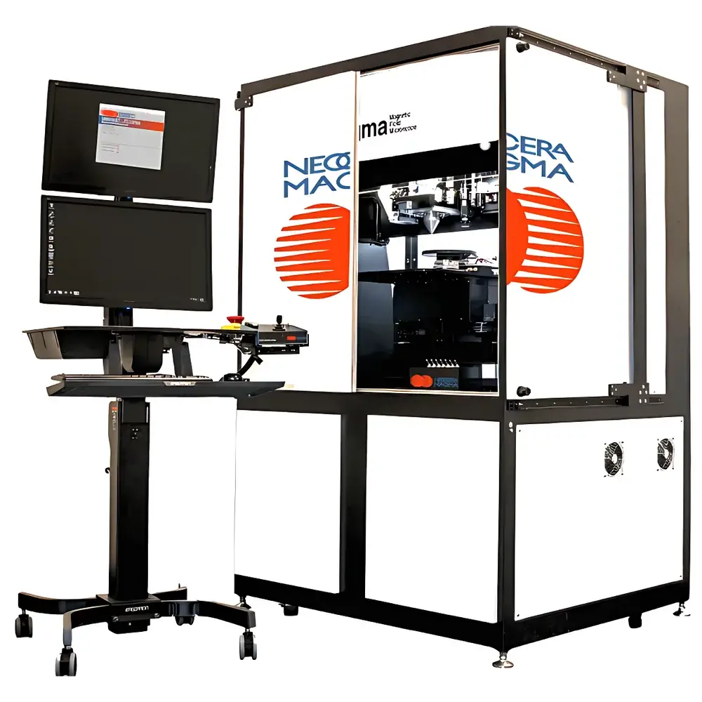
Neocera Magma EFI Magnetic Field Imaging Microscope System
| Brand | Neocera |
|---|---|
| Origin | USA |
| Manufacturer Type | Authorized Distributor |
| Origin Category | Imported |
| Model | Magma EFI |
| Pricing | Upon Request |
Overview
The Neocera Magma EFI Magnetic Field Imaging Microscope System is a high-precision, non-destructive failure analysis platform engineered for static defect localization in advanced semiconductor devices. Operating on the principle of magnetic field mapping—leveraging both superconducting quantum interference device (SQUID) magnetometry and scanning dielectric resonance (SDR) techniques—the system detects minute current-induced magnetic fields generated by fault currents (e.g., short circuits, leakage paths, or high-resistance opens) without physical contact or sample modification. Unlike conventional thermal or electrical probing methods, Magma EFI provides true 3D depth-resolved imaging through layered structures—including 3DICs, SiP packages, heterogeneous multi-chip modules (MCMs), and stacked-die assemblies—by correlating magnetic field gradients with current path geometry and penetration depth. Its dual-sensor architecture enables simultaneous high-sensitivity detection (sub-500 nA DC/AC) and sub-3 µm spatial resolution, making it uniquely suited for root-cause analysis at the die level, packaged IC level, and printed circuit board (PCB) level.
Key Features
- Integrated dual-mode sensing: SQUID-based DC–25 kHz magnetic field imaging for nanoscale current detection, and SDR-based RF resonance mapping (20–200 MHz) for high-depth open-circuit localization.
- High-fidelity spatial resolution: 3 µm lateral resolution with SQUID; 30 µm with SDR; optical alignment reference at 2 µm resolution (NIR/visible spectrum).
- Large-area scanning capability: Up to 100 mm × 100 mm scan area with automated stage positioning and Z-axis focus control.
- Non-invasive operation: No sample decapsulation, backside thinning, or voltage contrast required—enables analysis of fully assembled, hermetically sealed, or thermally sensitive devices.
- Multi-layer depth profiling: Magnetic field decay modeling and RF standing-wave phase analysis provide quantitative depth estimation up to 10 mm (SQUID) and <500 µm (SDR).
- Modular sensor configuration: HiRes tool combines SQUID and magnetoresistive (MR) sensors for concurrent sensitivity and spatial fidelity during current-scanning mode.
- Comprehensive signal generation: Bipolar function generator (±10 V / 100 mA, DC–200 kHz) supports controlled stimulus injection for fault activation and current path verification.
Sample Compatibility & Compliance
The Magma EFI accommodates a broad range of semiconductor packaging formats: bare dies on 300 mm wafers, final-package ICs (QFN, BGA, WLCSP, fan-out), PCBs up to A4 size, and complex heterogeneous integration platforms such as 2.5D/3D ICs, chiplets, and advanced SiP assemblies. All measurements comply with non-destructive testing (NDT) principles defined in ASTM E2375 and ISO 17025-accredited laboratory practices. The system supports GLP/GMP-aligned workflows via audit-trail-enabled software logging and meets essential electromagnetic compatibility (EMC) requirements per FCC Part 15 and IEC 61000-6-3. While not FDA-regulated, its traceable measurement chain aligns with analytical instrument qualification (AIQ) frameworks used in semiconductor reliability labs under ISO/IEC 17025.
Software & Data Management
Controlled via Windows 10 64-bit host software, the Magma EFI platform delivers synchronized acquisition, real-time magnetic field visualization, and multi-modal data fusion (magnetic + optical + CAD overlay). The software includes automated defect scoring algorithms, cross-sectional depth reconstruction tools, and export-ready reporting in CSV, TIFF, and industry-standard GDSII-compatible formats. Data integrity is maintained through timestamped metadata embedding, user-access controls, and optional 21 CFR Part 11-compliant electronic signature modules for regulated environments. Raw sensor data streams are preserved in HDF5 format for post-processing using MATLAB, Python (SciPy/NumPy), or custom finite-element modeling (FEM) workflows.
Applications
- Root-cause localization of static defects: shorts, leakage paths, resistive opens (>100 kΩ), and floating nodes in advanced nodes (≤5 nm) and wide-bandgap power devices.
- Failure analysis of stacked-die memory (HBM, DRAM stacks), interposer-based ASICs, and heterogeneous compute modules where traditional OBIRCH or TIVA are ineffective.
- Verification of design-for-test (DFT) structures, bond wire integrity, and redistribution layer (RDL) continuity in fan-out wafer-level packaging (FO-WLP).
- Qualification of underfill voids, solder joint cracks, and TIM delamination via secondary magnetic field perturbation signatures.
- Support for JEDEC JESD22-A114 (ESD), JESD22-A108 (HTOL), and JEP122 (failure mechanism modeling) test correlation studies.
FAQ
What types of defects can Magma EFI detect that conventional e-beam or optical methods cannot?
Magma EFI detects static current anomalies without requiring electron beam stimulation or optical access—making it effective for buried interconnects, metal layers under passivation, and fully encapsulated packages where OBIRCH, TIVA, or LADA fail.
Is cryogenic cooling required for SQUID operation?
Yes—the SQUID sensor operates at liquid helium temperatures (4.2 K); the system integrates a closed-cycle cryocooler with automated refill management and thermal stability monitoring.
Can Magma EFI be integrated into an existing FA lab workflow?
Yes—it supports standard SEM/FIB coordinate transfer protocols, CAD-to-image registration via fiducial markers, and direct import of ODB++, Gerber, and GDSII design files.
Does the system support AC current mapping?
Yes—SQUID mode supports frequencies from DC to 25 kHz; SDR mode operates from 20 MHz to 200 MHz, enabling both low-frequency leakage and high-frequency resonance-based open detection.
What is the typical turnaround time for a full die-level analysis?
Average scan time for a 10 mm × 10 mm region at 3 µm resolution is ~45 minutes; automated ROI targeting and multi-frequency sweeps reduce total FA cycle time by >60% compared to iterative probing methods.


