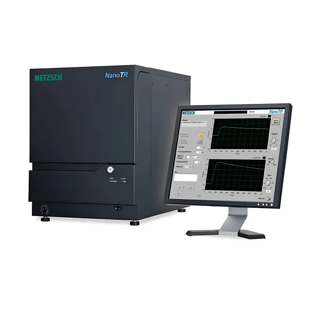
NETZSCH NanoTR Thermal Reflectance Analyzer
| Brand | NETZSCH |
|---|---|
| Origin | Germany |
| Model | NanoTR |
| Measurement Principle | Laser-based Thermal Reflectance (Time-Domain Thermoreflectance, TDTR) |
| Instrument Type | Thin-Film Thermal Conductivity Analyzer |
| Temperature Range | Ambient (RT) to 300 °C (optional heating stage) |
| Sample Dimensions | 10 × 10 mm to 20 × 20 mm |
| Film Thickness Range | 30 nm to 20 µm (dependent on material and measurement mode) |
| Thermal Diffusivity Range | 0.01 to 1000 mm²/s |
| Thermal Conductivity Range | 0.1 to 2000 W/(m·K) |
| Accuracy | ±5% |
| Repeatability | ±5% |
| Pulse Width | 1 ns |
| Probe Beam Diameter | 100 µm |
| Pump Laser Power | 100 mW |
| Measurement Modes | RF (Rear-Heating/Forward-Detection) and FF (Front-Heating/Forward-Detection) |
| Footprint (L×W×H) | 600 mm × 500 mm × 700 mm |
| Compliance | ISO 13826, ASTM E1461 (adapted for thin-film extension), NIST-traceable calibration protocols |
Overview
The NETZSCH NanoTR Thermal Reflectance Analyzer is a high-precision, laboratory-grade instrument engineered for non-contact, nanoscale thermal property characterization of thin films deposited on substrates. It implements time-domain thermoreflectance (TDTR)—a pump-probe laser technique—where a modulated pump laser pulse induces localized transient heating at the film–substrate interface, and a time-delayed probe beam detects minute changes in surface reflectivity correlated with thermal diffusion dynamics. Unlike conventional laser flash analysis (LFA), which assumes bulk homogeneity and semi-infinite geometry, the NanoTR resolves interfacial thermal resistance (Rth), cross-plane thermal conductivity (k⊥), thermal diffusivity (α), and volumetric heat capacity (ρcp) with sub-micron spatial resolution and picosecond temporal sensitivity. Designed for R&D laboratories in semiconductor process development, advanced packaging, MEMS/NEMS fabrication, and next-generation thermal interface materials (TIMs), the NanoTR delivers quantitative, physics-based thermal transport data essential for modeling phonon scattering, interfacial Kapitza resistance, and size effects in nanolayered systems.
Key Features
- True TDTR architecture with synchronized femtosecond-class timing electronics and dual-path optical delay line for precise phase-resolved detection
- Dual operational modes: RF (Rear-Heating/Forward-Detection) for opaque substrate configurations and FF (Front-Heating/Forward-Detection) for transparent or semi-transparent stacks
- Integrated temperature-controlled stage supporting ambient-to-300 °C operation with ±0.5 °C stability, enabling thermal conductivity vs. temperature profiling
- Automated beam alignment and focus optimization via motorized XYZ stages and real-time reflectivity feedback
- NIST-traceable calibration routines compliant with ISO/IEC 17025 requirements; includes certified reference standards for SiO2/Si, Al/Si, and Au/Si bilayers
- Robust mechanical design with vibration-damped optical table integration and EMI-shielded enclosure for stable long-term acquisition
Sample Compatibility & Compliance
The NanoTR accommodates rigid planar samples up to 20 × 20 mm with thicknesses from 0.3 mm to 5 mm. Compatible film systems include sputtered or evaporated metals (e.g., Cu, Al, TiN), atomic-layer-deposited dielectrics (e.g., Al2O3, HfO2), spin-coated polymers (e.g., polyimide, BCB), and 2D materials (e.g., graphene, MoS2) on Si, SiO2, sapphire, or quartz substrates. All measurements adhere to metrological best practices outlined in ISO 13826 (Thermal conductivity of thin films by optical methods) and are compatible with GLP-compliant workflows. Data integrity is ensured through full audit trails, electronic signatures, and 21 CFR Part 11–ready software configuration options.
Software & Data Management
The NanoTR operates under NETZSCH’s proprietary ThermoReflect™ v4.x platform—a Windows-based application offering real-time signal visualization, multi-parameter curve fitting (using analytical solutions to the 1D heat diffusion equation with interfacial boundary conditions), and batch processing for statistical repeatability assessment. Raw oscilloscope traces, demodulated lock-in signals, and fitted thermal parameters are stored in HDF5 format with embedded metadata (sample ID, operator, timestamp, environmental conditions). Export options include CSV, MATLAB .mat, and PDF reports conforming to internal QA templates. Optional API access enables integration into automated test benches and LIMS environments.
Applications
- Quantifying cross-plane k⊥ of high-k dielectric barriers in advanced logic nodes (e.g., <10 nm Al2O3 on Si)
- Evaluating thermal boundary resistance at metal–semiconductor interfaces in power devices
- Characterizing anisotropic thermal transport in vertically aligned CNT or graphene composite films
- Validating TCAD thermal models used in electrothermal simulation of GaN HEMTs and SiC MOSFETs
- Screening thermal performance of low-κ polymer interlayer dielectrics under thermal cycling
- Supporting DOE studies for ALD process optimization via thermal property–thickness correlations
FAQ
What is the minimum detectable film thickness?
The practical lower limit is ~30 nm for high-contrast metal-on-semiconductor systems (e.g., Al/Si); it increases to ~200 nm for low-contrast polymer-on-glass configurations due to signal-to-noise constraints.
Can the NanoTR measure anisotropic thermal conductivity?
No—the standard configuration measures only cross-plane (z-direction) thermal transport. In-plane (x/y) anisotropy requires complementary techniques such as scanning thermal microscopy (SThM) or micro-Raman thermography.
Is vacuum or inert gas environment required?
Ambient air operation is fully supported; optional purge ports allow N2 or Ar purging to minimize convective artifacts during elevated-temperature measurements.
How is calibration performed?
Calibration employs certified reference samples with known thermal properties traceable to NIST Standard Reference Materials (SRMs); system response is validated before each measurement series using built-in photodiode monitoring and reference reflectivity checks.
Does the software support automated pass/fail criteria for QC workflows?
Yes—customizable acceptance thresholds can be defined per parameter (e.g., k⊥ ±3%, Rth < 5×10⁻⁸ m²·K/W); deviations trigger visual alerts and log entries with root-cause tagging.


