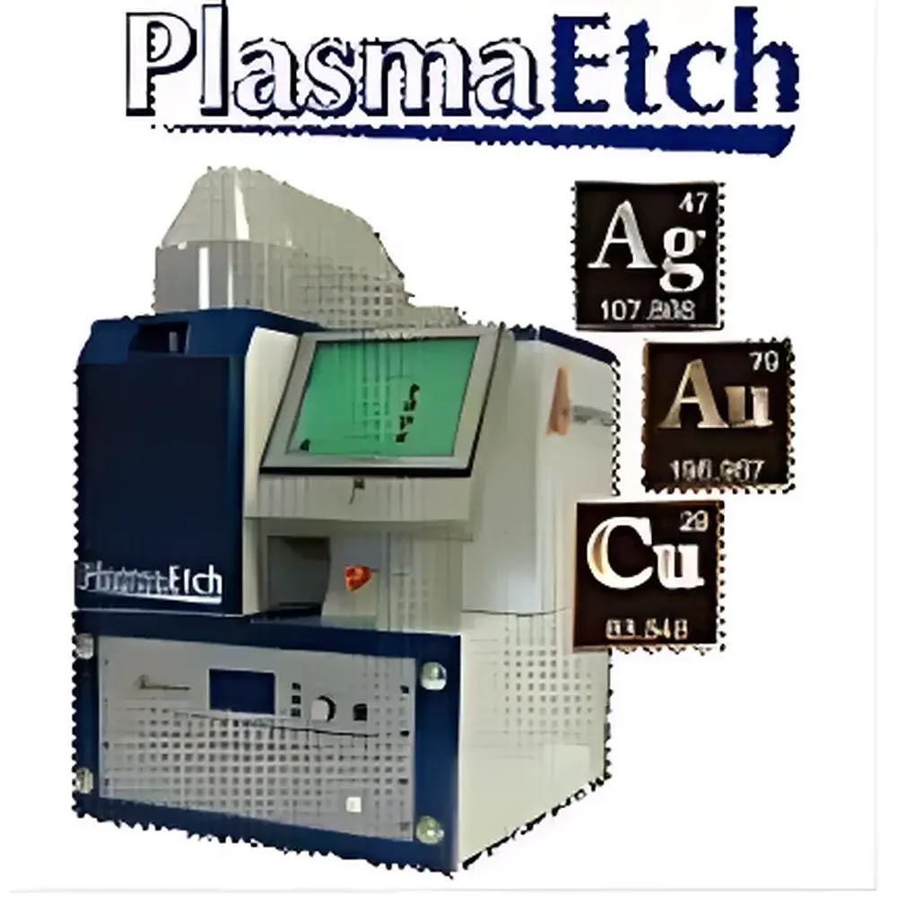
Nisene PlasmaEtch Microwave-Induced Plasma Decapsulation System
| Brand | Nisene |
|---|---|
| Origin | USA |
| Model | PlasmaEtch |
| Technology | Microwave-induced plasma etching |
| Patent | US Patent 9,548,227 B2 |
| Compliance | RoHS-compliant process, halogen-free etchant chemistry |
| Application | Semiconductor IC decapsulation for failure analysis (FA), cross-sectioning, and package-level defect inspection |
Overview
The Nisene PlasmaEtch is a fully automated, microwave-induced plasma decapsulation system engineered for high-precision, non-destructive removal of epoxy mold compound (EMC) and other polymer-based encapsulants from integrated circuits (ICs) and advanced semiconductor packages. Unlike conventional wet chemical or mechanical methods, the PlasmaEtch utilizes a controlled microwave-generated plasma discharge within a sealed quartz tube to selectively oxidize organic encapsulant materials into volatile byproducts (e.g., CO₂, H₂O, NOₓ), leaving underlying metal interconnects—including copper bond wires, silver sintered die-attach, and aluminum metallization—intact and unaltered. This physical-chemical etching mechanism enables reproducible, operator-independent decapsulation with sub-micron depth control, eliminating risks of wire sweep, pad corrosion, or thermal damage associated with acid boiling or laser ablation. Designed for integration into Class 1000 cleanroom environments, the system supports FA labs requiring ISO/IEC 17025-compliant workflows and GLP-aligned documentation.
Key Features
- Microwave-induced plasma generation (2.45 GHz) with real-time RF power modulation (50–300 W range) for tunable etch rate and selectivity
- Patented plasma discharge tube geometry (US Patent 9,548,227 B2) ensuring uniform plasma distribution across sample surface up to 100 mm × 100 mm
- Integrated vacuum manifold with dual-stage pumping (rotary vane + turbomolecular) maintaining base pressure <5 × 10⁻³ mbar for stable plasma ignition
- Programmable multi-step etch protocols with independent control of gas flow (O₂, CF₄, Ar mixtures), dwell time, and power ramp profiles
- Automated sample stage with XYZ positioning and Z-height sensing for repeatable focal plane alignment
- Onboard optical monitoring via integrated CCD camera and LED ring illumination for in-situ visual verification of etch progress
- Touchscreen HMI with password-protected user roles (Operator, Technician, Administrator) and audit-trail logging per FDA 21 CFR Part 11 requirements
Sample Compatibility & Compliance
The PlasmaEtch accommodates a broad spectrum of modern packaging architectures, including QFN, BGA, WLCSP, Fan-Out Wafer-Level Packages (FOWLP), and 2.5D/3D stacked die assemblies. It is validated for decapsulating leadframe-based devices with Cu, Au, and Ag bond wires; flip-chip solder bumps (SnAg, SAC305); and low-k dielectric layers (SiCOH, porous silica). All process chemistries are halogen-free and RoHS-compliant, generating no hazardous waste streams requiring special disposal—eliminating need for acid neutralization tanks or fume scrubbers. The system meets SEMI S2/S8 safety standards and supports traceability documentation required for ISO 9001 and IATF 16949-certified FA laboratories.
Software & Data Management
Controlled by Nisene’s proprietary DecapSuite™ v4.2 software, the PlasmaEtch provides full protocol management, parameter versioning, and electronic batch records (EBR). Each run generates timestamped metadata—including chamber pressure history, RF forward/reflected power logs, gas composition traces, and annotated optical frames—exportable as CSV or PDF for inclusion in FA reports. Software supports secure network deployment with TLS 1.2 encryption, LDAP authentication, and configurable retention policies aligned with internal QA data governance frameworks. Optional IQ/OQ/PQ validation packages are available to support GMP-regulated environments.
Applications
- Failure analysis of parametric failures (leakage, IDDQ anomalies) requiring die surface access without interconnect damage
- Verification of underfill voids, delamination, or mold compound cracking in automotive and aerospace-grade ICs
- Preparation for FIB-SEM cross-sectioning and TEM lamella extraction
- Root-cause investigation of electrochemical migration (ECM) or corrosion-related field returns
- Qualification of new encapsulant formulations during package development
- Support for JEDEC JESD22-A108 humidity testing follow-up analysis
FAQ
Does the PlasmaEtch process affect copper or silver bond wires?
No. The oxidative plasma chemistry selectively targets carbon-hydrogen-oxygen bonds in polymers while exhibiting negligible reactivity toward metallic conductors. Independent SEM-EDS studies confirm no measurable Cu oxidation or Ag sulfidation after standard etch cycles.
What is the typical etch rate for standard EMC?
Under optimized O₂/CF₄ plasma conditions, average etch rates range from 15–25 µm/min for standard FR-4-compatible EMC, with ±0.8 µm run-to-run repeatability (n=30, 3σ).
Can the system handle stacked-die or TSV packages?
Yes. The Z-height auto-sensing feature and programmable depth-stop functionality enable sequential layer-by-layer decapsulation of heterogeneous stacks, including silicon interposers and through-silicon vias.
Is regulatory validation support available?
Yes. Nisene provides IQ/OQ documentation templates, calibration certificates traceable to NIST standards, and on-site PQ execution support for labs operating under FDA, ISO 13485, or AEC-Q200 compliance mandates.


