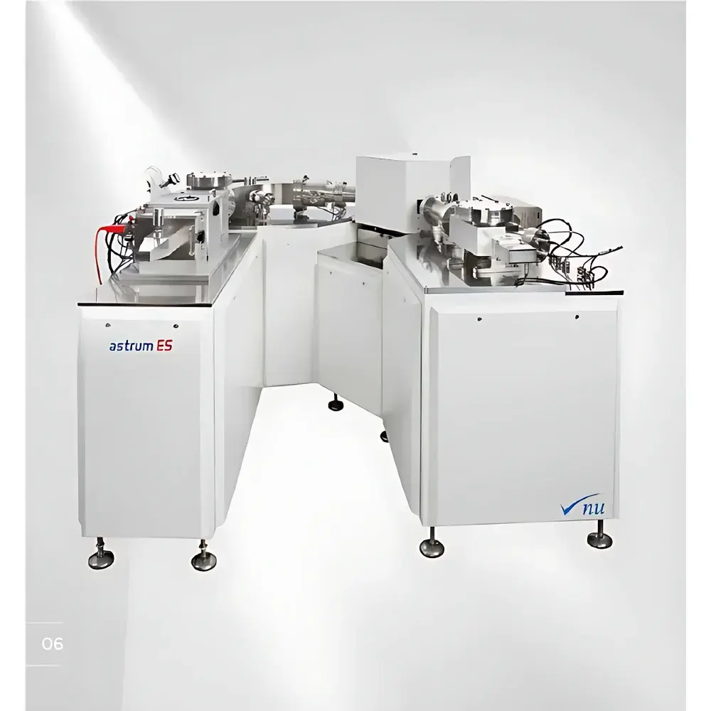
NU Astrum ES Dual-Focusing Glow Discharge Mass Spectrometer
| Brand | NU |
|---|---|
| Origin | United Kingdom |
| Manufacturer Type | Authorized Distributor |
| Origin Category | Imported Instrument |
| Model | Astrum ES |
| Pricing | Available Upon Request |
Overview
The NU Astrum ES is a high-performance dual-focusing glow discharge mass spectrometer (GD-MS) engineered for ultra-trace elemental analysis of solid conductive and semi-conductive materials. Operating on the principle of low-pressure argon plasma sputtering coupled with magnetic sector mass separation, the Astrum ES enables direct solid sampling without dissolution or matrix-matched calibration. Its double-focusing geometry—comprising an electrostatic analyzer (ESA) and a magnetic sector—delivers high mass resolution (M/ΔM > 8,000), excellent mass accuracy (< 2 ppm), and exceptional signal-to-noise ratios essential for sub-ppt detection limits. Designed specifically for demanding applications in high-purity material certification, the instrument achieves quantitative multi-element analysis across the full periodic table—from lithium to uranium—in a single acquisition, with dynamic quantification spanning over 10 orders of magnitude (sub-ppb to major constituent levels).
Key Features
- Dual-focusing magnetic sector mass analyzer with adjustable ion optics for optimized transmission and resolution
- High-stability radiofrequency (RF) and direct-current (DC) glow discharge source compatible with both conductive and insulating samples (e.g., SiO₂, Al₂O₃, doped semiconductors)
- Multi-collector array with Faraday cups and discrete-dynode electron multipliers for simultaneous isotope detection and high-precision ratio measurements
- Integrated vacuum system featuring turbomolecular pumping stages and cryo-trapping for ultra-low background Ar⁺ and H₂O interference
- Automated sample introduction carousel supporting up to 24 standardized 1-inch diameter discs with reproducible positioning and sputter rate calibration
- Rugged, modular architecture compliant with ISO 17025 laboratory infrastructure requirements and designed for 24/7 operation in regulated environments
Sample Compatibility & Compliance
The Astrum ES accepts flat, polished solid samples up to 25 mm in diameter and 10 mm in thickness—including single-crystal silicon wafers, titanium alloys, copper refinery cathodes, nickel-based superalloys, and sintered ceramic substrates. Sample surface roughness must be ≤ 0.1 µm Ra for stable discharge and quantitative sputtering. The system meets ASTM E2923–22 for GD-MS performance verification and supports traceable calibration via NIST SRM 2136 (high-purity copper) and BAM CRM 115a (silicon). Full audit trail functionality complies with FDA 21 CFR Part 11 and EU Annex 11 requirements when operated with Nu’s certified software suite, enabling GLP/GMP-aligned reporting for semiconductor fab QC labs and aerospace material qualification centers.
Software & Data Management
Controlled by Nu’s proprietary NuScript™ v4.2 platform, the Astrum ES provides method-driven acquisition, real-time spectral visualization, and automated peak integration using centroid and profile-fitting algorithms. Data processing includes internal standard normalization (e.g., using matrix isotope signals), inter-element sensitivity correction via relative sensitivity factors (RSFs), and isotopic abundance correction for polyatomic interferences (e.g., ⁴⁰Ar¹⁶O⁺ on ⁵⁶Fe⁺). All raw and processed datasets are stored in vendor-neutral .mzML format, supporting third-party chemometric tools such as MATLAB® and Python-based SciPy workflows. Software validation documentation—including IQ/OQ/PQ protocols—is available upon request for regulated laboratories undergoing ISO/IEC 17025 accreditation.
Applications
- Quantitative impurity profiling of electronic-grade silicon (>99.9999999% purity) for IC manufacturing process control
- Trace element mapping in additively manufactured Ti-6Al-4V turbine blades to assess powder feedstock contamination
- Depth-resolved analysis of thin-film photovoltaic absorber layers (e.g., CIGS) via controlled sputter time calibration
- Certification of reference materials for national metrology institutes (NMIs) under ISO Guide 35
- Forensic metallurgical analysis of recovered spacecraft components following orbital exposure
FAQ
What sample preparation is required prior to GD-MS analysis on the Astrum ES?
Samples must be mechanically polished to mirror finish (≤ 0.1 µm Ra), ultrasonically cleaned in high-purity acetone and methanol, and dried under class-100 nitrogen flow. No acid etching or conductive coating is needed.
Can the Astrum ES analyze non-conductive materials such as fused silica or YSZ ceramics?
Yes—using RF mode operation at 13.56 MHz, the instrument sustains stable plasma on dielectric substrates; optional RF impedance matching network ensures optimal power coupling and sputter yield reproducibility.
How does the Astrum ES ensure long-term calibration stability for routine QC testing?
Daily automated tuning routines verify mass axis alignment and detector gain; quarterly RSF recalibration against matrix-matched CRMs maintains quantitative fidelity across instrument lifetime.
Is remote diagnostics and software update support available?
Yes—Nu’s SecureLink™ remote access protocol enables encrypted, audited technician intervention with customer approval and session logging per ISO/IEC 27001 standards.
Related Products

")