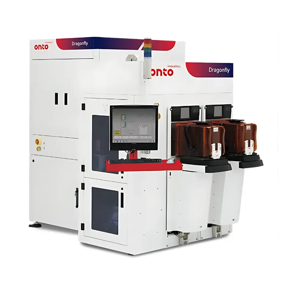
Onto Innovation Dragonfly® G3 Automatic Optical Inspection System for Semiconductor Wafers
| Brand | Onto Innovation |
|---|---|
| Model | Dragonfly® G3 |
| Origin | Malaysia |
| Equipment Type | Inline AOI for Front-End & Advanced Packaging |
| Minimum Detectable Line Width/Spacing | 0.7 µm |
| Wafer Size Support | 100 mm – 330 mm |
| Maximum Substrate Area | >6400 mm² |
| 翘曲晶圆 & Taiko Handling | Supported |
| Imaging Modes | Brightfield, Darkfield, Oblique Illumination, IR Transmission |
| 3D Metrology | Truebump® (Multi-Modal 3D Profilometry) |
| Residue Detection | Clearfind® |
| Software Platform | nLINE™ with Real-Time Analysis, Offline Review, and Exploratory Bump-Level Data Analytics |
| Compliance Framework | Supports ASTM F2598 (Wafer Defect Classification), ISO 14644-1 (Cleanroom Integration), and GLP/GMP-aligned Audit Trail Logging |
Overview
The Onto Innovation Dragonfly® G3 is a high-precision, dual-mode automatic optical inspection (AOI) system engineered specifically for semiconductor front-end manufacturing and advanced packaging applications. It employs a hybrid optical architecture integrating high-resolution 2D brightfield/darkfield imaging with multi-modal 3D surface profilometry—principally enabled by Onto Innovation’s proprietary Truebump® technology—to simultaneously detect sub-micron defects and quantify critical topographic features such as bump height, coplanarity, and solder volume. Unlike conventional AOI platforms limited to surface reflectivity contrast, the Dragonfly G3 leverages oblique illumination, infrared transmission imaging, and polarization-sensitive optics to resolve low-contrast anomalies in active pixel regions of CMOS image sensors (CIS), dielectric residues on redistribution layers (RDL), and micro-voids in underfill materials. Its modular sensor architecture supports real-time focus tracking across highly warped wafers—including Taiko-thinned substrates—ensuring metrological stability without mechanical recalibration. Designed for integration into 300 mm and larger substrate production lines, the system meets the stringent throughput, repeatability, and traceability requirements of ISO/IEC 17025-accredited fabs and FDA-regulated assembly facilities.
Key Features
- Sub-0.7 µm defect detection capability using optimized Köhler illumination and high-NA objective lenses with adaptive focus control
- Truebump® 3D metrology engine combining structured light, focus variation, and interferometric profiling for bump height accuracy ≤±0.15 µm (k=2) and coplanarity resolution <0.2 µm
- Clearfind® non-visual residue detection module enabling identification of organic/inorganic residues invisible under standard visible-light AOI
- nLINE™ software suite with native CAD data import, rule-based binning, and machine-learning-assisted classification (MLAC) trained on >10⁶ labeled defect instances
- Real-time alignment engine supporting wafer-level pattern matching without fiducial marks; compatible with maskless lithography reference data
- Fully programmable illumination sequencing—including multi-angle darkfield, polarized oblique, and NIR transmission—for application-specific contrast optimization
- Integrated IR inspection channel for subsurface void detection in through-silicon vias (TSVs) and embedded die stacks
Sample Compatibility & Compliance
The Dragonfly G3 accommodates substrates from 100 mm to 330 mm diameter, including full-wafer, panel-level, and cut-die formats. Its vacuum chuck and adaptive clamping system handle warpage up to ±3 mm P–V while maintaining Z-axis repeatability within ±0.3 µm. The platform complies with SEMI S2/S8 safety standards and integrates seamlessly into factory automation via SECS/GEM protocol. All measurement data are timestamped, user-attributed, and stored with cryptographic hashing to satisfy FDA 21 CFR Part 11 electronic record requirements. Process recipes and inspection logs support full audit trail generation per ISO 9001:2015 and IATF 16949 quality management frameworks. Calibration procedures follow NIST-traceable protocols aligned with ASTM F2598 for defect classification consistency across multiple toolsets.
Software & Data Management
The nLINE™ software provides unified control over acquisition, analysis, review, and reporting. Its distributed architecture separates real-time inspection tasks from offline exploratory analytics—enabling concurrent line operation and deep-dive bump-level statistical process control (SPC). The system generates hierarchical defect maps linked directly to design layout (GDSII/OASIS), allowing root-cause correlation between physical anomalies and layout hotspots. Raw image data are archived in TIFF-6.0 format with embedded EXIF metadata (exposure time, lens ID, calibration ID, stage position). For advanced yield learning, the platform exports structured JSON datasets compliant with Yield Explorer™ and PDF-2.0 semiconductor data interchange standards. Secure remote access is enabled via TLS 1.3-encrypted web interface with RBAC (role-based access control) and session timeout enforcement.
Applications
- Front-end defect monitoring: post-etch residue, photoresist scumming, gate oxide pinholes, and shallow trench isolation (STI) dishing
- Advanced packaging: copper pillar and micro-bump coplanarity assessment, underfill void detection, RDL cracking, and fan-out wafer-level packaging (FOWLP) alignment verification
- CMOS image sensor (CIS) inspection: active pixel region defects (e.g., microlens misalignment, color filter bleed, pixel crosstalk artifacts)
- Heterogeneous integration: die-to-wafer bonding defect classification, TSV opening inspection, and interposer bridge integrity validation
- Compound semiconductor substrates: GaN-on-Si and SiC wafer surface defect mapping with thermal drift compensation
FAQ
Does the Dragonfly G3 support automated recipe generation from CAD layout files?
Yes—the system accepts GDSII, OASIS, and DXF inputs to auto-generate inspection zones, exclusion masks, and focus map templates without manual coordinate entry.
Can it inspect wafers with >2 mm total indicator reading (TIR) warpage?
Yes—its dynamic focus tracking and vacuum-assisted substrate leveling enable stable imaging on wafers with up to ±3 mm P–V warpage, including Taiko-ground substrates.
Is Truebump® 3D metrology validated against NIST-traceable step-height standards?
Yes—calibration is performed using NIST SRM 2160 and NIST SRM 2161 reference artifacts, with annual verification documented per ISO/IEC 17025 clause 6.6.
What data security protocols are implemented for electronic records?
All inspection logs include digital signatures, immutable timestamps, and AES-256 encryption at rest and in transit, satisfying FDA 21 CFR Part 11 §11.10 and EU Annex 11 requirements.
How does Clearfind® differentiate between benign particles and process-critical residues?
Clearfind® uses spectral reflectance modeling combined with multi-wavelength scattering analysis to classify residue composition (e.g., photoresist vs. metal oxide) with >92% specificity in controlled environment testing.


