ONYX-1 Graphene & 2D Materials Non-Contact Electrical Characterization System by Das-Nano
| Brand | Das-Nano |
|---|---|
| Origin | USA |
| Model | ONYX-1 |
| Instrument Type | Room-Temperature Hall Effect System |
| Current Source Range | 20 mA |
| Measurement Principle | Microwave Reflectometry-Based Carrier Profiling |
| Applicable Mobility Range | 100–3000 cm²/V·s |
| Sample Compatibility | Monolayer to multilayer graphene, graphene oxide, PEDOT:PSS, CNT dispersions, MoS₂, h-BN, ALD-ZnO, GaN-on-SiC epiwafers, spin-coated photoresists, powders, and inkjet-printed films |
Overview
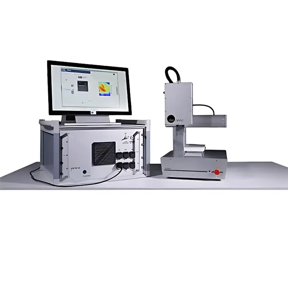
The ONYX-1 Non-Contact Electrical Characterization System, developed by Das-Nano (USA), is an industrial-grade metrology platform engineered for rapid, non-destructive quantification of sheet resistance (Rs), carrier concentration (ns), and Hall mobility (µ) in two-dimensional (2D) semiconducting materials. Unlike conventional contact-based Hall effect systems that require metalized van der Pauw contacts and cryogenic cooling, the ONYX-1 employs microwave reflectometry—specifically, frequency-domain resonant cavity perturbation—to extract electrical parameters without physical probe contact. This physics-based approach eliminates contact resistance artifacts, avoids surface damage or contamination, and enables direct measurement on as-fabricated wafers, patterned devices, or fragile layered structures. The system operates at ambient temperature and pressure, making it suitable for inline process monitoring in R&D cleanrooms and pilot-line fabs. Its design adheres to the fundamental constraints of high-frequency electromagnetic interaction with conductive thin films, where shifts in resonant frequency and quality factor (Q) correlate directly with sheet conductivity and carrier scattering time.
Key Features
- Non-contact, non-invasive characterization: No lithographic patterning or metallization required; measurements performed through air or inert gas environments.
- Single-point and full-area mapping capability: Motorized XY stage supports automated raster scanning up to 300 mm wafers (standard); resolution down to 50 µm per pixel.
- High throughput: Typical acquisition time of <15 seconds per point; full 200-mm wafer map completed in under 30 minutes.
- Calibration traceability: Factory-calibrated using NIST-traceable Si reference wafers; software includes built-in drift compensation algorithms for long-term stability.
- Robust architecture: RF-shielded enclosure minimizes EMI interference; temperature-stabilized cavity ensures measurement repeatability within ±2% Rs and ±3% µ across 8-hour sessions.
- Integrated environmental control option: Optional dry nitrogen purge or vacuum chamber interface for oxygen/moisture-sensitive samples (e.g., freshly exfoliated flakes).
Sample Compatibility & Compliance
The ONYX-1 is validated for use with a broad spectrum of emerging 2D and low-dimensional semiconductor systems, including but not limited to: monolayer and bilayer graphene on SiO2/Si and hexagonal boron nitride substrates; chemical vapor deposition (CVD) graphene films; solution-processed graphene oxide and reduced GO; PEDOT:PSS thin films; transition metal dichalcogenides (MoS2, WS2, WSe2); epitaxial GaN and AlGaN on SiC; atomic layer deposited (ALD) ZnO and ITO; spin-coated photoresists; and nanomaterial inks (CNT, AgNW). All measurements comply with ASTM F394-22 (Standard Practice for Sheet Resistance Measurements of Thin Conductive Films Using Microwave Resonance) and support GLP/GMP documentation workflows. Audit trails, user access logs, and electronic signatures are enabled via optional FDA 21 CFR Part 11-compliant software module.
Software & Data Management
ONYX Control Suite v4.2 provides a deterministic, scriptable interface for instrument control, data acquisition, and parameter extraction. The software implements proprietary inverse modeling algorithms based on rigorous electromagnetic field solutions of the TE011 cavity mode perturbed by thin-film conductivity tensors. Raw S-parameter data (S11) is stored in HDF5 format with embedded metadata (timestamp, operator ID, environmental conditions, calibration state). Batch processing supports statistical analysis per lot, spatial uniformity heatmaps, trend charting over time, and export to CSV, MATLAB (.mat), or industry-standard SEMI E142 (Equipment Data Acquisition) format. Integration with MES/SPC platforms is achieved via OPC UA or RESTful API endpoints.
Applications
- R&D optimization of CVD graphene growth parameters (temperature, pressure, precursor flow) via real-time sheet resistance feedback.
- In-process verification of ALD ZnO thickness and doping uniformity across 200-mm display backplane substrates.
- Quality screening of MoS2 monolayers transferred onto target dielectrics prior to FET fabrication.
- Quantitative assessment of PEDOT:PSS film degradation under thermal stress or UV exposure.
- Correlation of inkjet-printed carbon nanotube network morphology (via AFM) with bulk sheet resistance maps from ONYX-1.
- Process window definition for plasma-enhanced atomic layer deposition (PE-ALD) of NbCIZO transparent conductors.
FAQ
Does the ONYX-1 require sample patterning or electrode deposition?
No. The system performs fully non-contact measurements and does not require van der Pauw geometry or any metallization.
Can it measure insulating or highly resistive 2D layers?
The ONYX-1 is optimized for conductive and semi-conductive 2D materials with sheet resistance ranging from 10 Ω/sq to 10 kΩ/sq. Insulators (Rs > 1 MΩ/sq) fall outside its dynamic range.
Is calibration needed before each measurement session?
A daily warm-up and cavity resonance check are recommended; full recalibration is required only after hardware maintenance or every 6 months per ISO/IEC 17025 guidelines.
How is carrier type (n vs. p) determined?
The ONYX-1 measures magnitude only. Polarity must be inferred from complementary techniques (e.g., Seebeck coefficient, transfer curve hysteresis) or known material band structure.
What substrates are compatible?
Standard configurations support Si/SiO2, sapphire, quartz, and flexible PET; custom fixtures available for irregular geometries or thick ceramics.