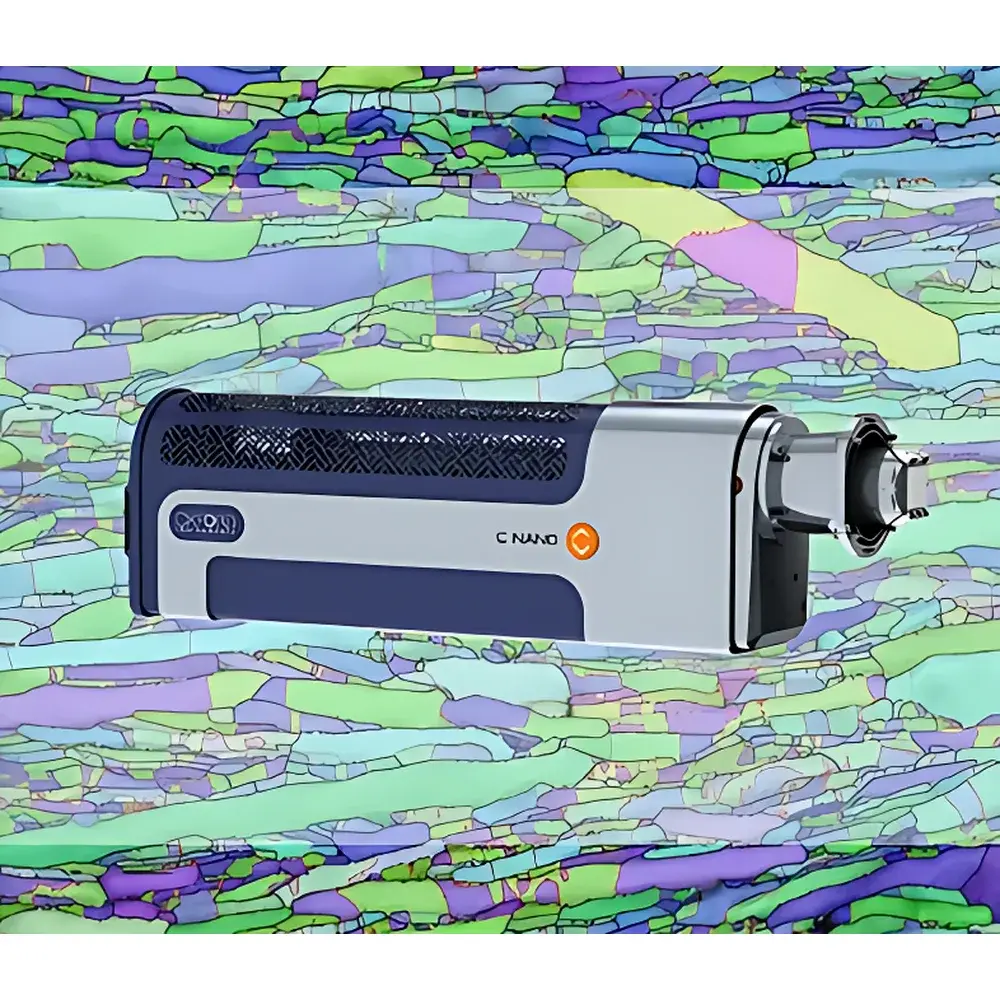
Oxford Instruments C-Nano EBSD Detector for SEM
| Brand | Oxford Instruments |
|---|---|
| Origin | United Kingdom |
| Model | C-Nano |
| CCD Camera Resolution | 1244 × 1024 pixels |
| Maximum Pattern Acquisition Rate | 870 Hz |
| Spatial Resolution | 2 nm |
| Angular Resolution | < 0.05° |
Overview
The Oxford Instruments C-Nano EBSD Detector is a high-performance, entry-level electron backscatter diffraction (EBSD) system engineered specifically for integration with scanning electron microscopes (SEM). It leverages proprietary CMOS sensor architecture and advanced optical design to deliver exceptional sensitivity, speed, and angular fidelity—critical parameters for quantitative microstructural characterization at the nanoscale. Unlike legacy CCD-based detectors, the C-Nano employs a custom-designed back-illuminated CMOS sensor optimized for low-dose, high-speed pattern acquisition. Its operation relies on the formation of Kikuchi bands from inelastically scattered electrons within the interaction volume of crystalline samples under incident electron beam irradiation; these bands are captured, indexed, and analyzed to determine crystallographic orientation, phase identification, grain boundary character, and lattice strain distribution with sub-micron spatial registration.
Key Features
- High-speed pattern acquisition up to 870 Hz—enabling rapid mapping of large fields-of-view without compromising data integrity
- Full-frame high-resolution EBSD patterns at 1244 × 1024 pixels for advanced strain analysis and defect characterization
- Optimized low-beam-current performance: reliable indexing at beam currents below 3 nA, essential for beam-sensitive materials including polymers, ceramics, and nanocrystalline alloys
- Sub-pixel geometric distortion correction enabled by precision optics, ensuring angular resolution better than 0.05°—a prerequisite for accurate misorientation and elastic strain quantification per ASTM E3039 and ISO/IEC 17025-compliant workflows
- Integrated proximity sensor with automatic retraction mechanism safeguards both detector and SEM column during stage movement or tilt adjustments
- Waveform-compatible bellows interface maintains ultra-high vacuum integrity (<1 × 10⁻⁶ mbar) in modern field-emission SEM platforms
- Native synchronization with Oxford Instruments’ AZtecCrystal software suite for concurrent EDS-EBSD acquisition and correlative microanalysis
Sample Compatibility & Compliance
The C-Nano is validated for use across diverse material classes—including metals, intermetallics, geological specimens, semiconductor wafers, and advanced composites—without requiring conductive coating in many cases due to its high quantum efficiency. It supports routine analysis under standard SEM operating conditions (10–30 kV acceleration voltage, working distances of 10–20 mm), and is compatible with both tungsten and field-emission gun (FEG) sources. All hardware and firmware comply with CE marking requirements and electromagnetic compatibility (EMC) Directive 2014/30/EU. Data acquisition protocols adhere to GLP/GMP-aligned audit trail functionality when used with AZtec software configured for FDA 21 CFR Part 11 compliance.
Software & Data Management
The C-Nano operates exclusively through Oxford Instruments’ AZtecCrystal platform—a modular, scriptable environment supporting automated calibration, dynamic background subtraction, confidence index filtering, and grain reconstruction using Hough-transform-based indexing. Raw pattern datasets are stored in standardized HDF5 format, enabling interoperability with third-party tools such as MTEX and EMsoft. Batch processing pipelines support parallelized indexing across multi-core CPUs, while GPU-accelerated band detection improves throughput for large-area maps (>10⁶ points). Metadata embedding includes full traceability of acquisition parameters (beam energy, dwell time, step size, tilt angle), facilitating reproducibility in inter-laboratory studies aligned with ISO 11888 and ASTM E112 standards.
Applications
- Quantitative texture analysis in rolled aluminum alloys and titanium sheet products
- Nanograin boundary engineering in additively manufactured Ni-based superalloys
- Phase transformation mapping in heat-treated steels and duplex stainless steels
- Strain gradient evaluation near crack tips and weld interfaces via high-resolution pattern shift analysis
- Crystallographic orientation imaging of battery cathode particles (e.g., NMC, LFP) under low-kV conditions
- Geological provenance studies using detrital zircon EBSD coupled with CL and EDS
FAQ
What is the minimum beam current required for stable indexing with the C-Nano?
Stable indexing is routinely achieved at beam currents as low as 2.5 nA under optimal sample preparation and geometry conditions.
Does the C-Nano support simultaneous EDS-EBSD acquisition?
Yes—native hardware synchronization enables real-time, pixel-registered acquisition with Oxford Instruments’ X-MaxN or Ultim Max EDS detectors.
Can the C-Nano be retrofitted onto older SEM models?
It is compatible with most modern SEMs equipped with standard EBSD ports (e.g., FEI/Thermo Scientific, Zeiss, JEOL, Hitachi); retrofit feasibility requires vacuum port diameter verification and controller compatibility assessment.
Is the 1244 × 1024 pattern resolution usable for strain analysis?
Yes—this full-resolution mode provides sufficient sampling density for sub-pixel cross-correlation algorithms used in high-fidelity elastic strain mapping per ISO/IEC 17025-accredited laboratories.
How does the proximity sensor interface with the SEM control system?
It communicates via TTL-level signals over a dedicated I/O port, triggering automatic detector retraction upon detection of stage or pole piece encroachment—no additional software layer required.


