Oxford Instruments NA-TKD Electron Backscatter Diffraction System
| Brand | Oxford Instruments |
|---|---|
| Origin | United Kingdom |
| Model | NA-TKD |
| Compatibility | Fully compatible with Oxford Instruments Symmetry CMOS EBSD detectors |
| Configuration | Near-axis phosphor screen geometry |
| Primary Application | High-resolution crystallographic orientation and strain mapping in thin, beam-sensitive, or nanoscale materials |
Overview
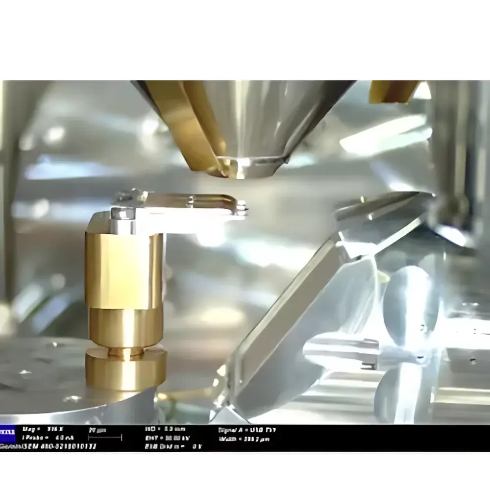
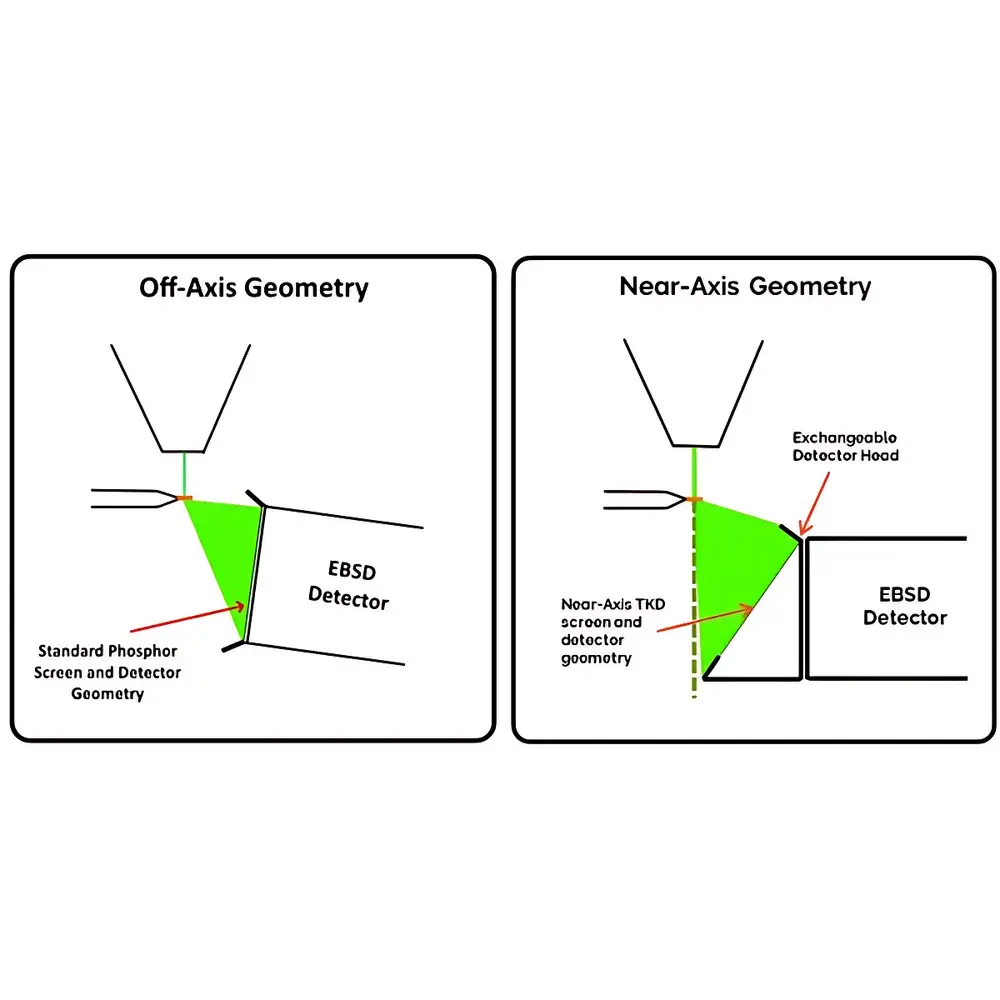
The Oxford Instruments NA-TKD (Near-Axis Transmission Kikuchi Diffraction) system is a high-performance electron backscatter diffraction solution engineered for advanced crystallographic characterization in scanning electron microscopes (SEM). Unlike conventional off-axis TKD (OA-TKD), NA-TKD positions the phosphor screen in close proximity to the primary electron beam axis—enabling significantly enhanced signal collection efficiency without compromising geometric fidelity. This near-axis geometry leverages optimized electron trajectory paths to maximize diffraction pattern intensity while minimizing pattern distortion, resulting in up to 10× improvement in spatial resolution and detection sensitivity compared to standard OA-TKD configurations. The system operates under typical SEM conditions: short working distance (~3–5 mm), high accelerating voltage (15–30 kV), and low probe current (sub-pA to few pA), making it especially suitable for characterizing ultra-thin TEM lamellae, ion-milled cross-sections, nanograined alloys, and radiation-sensitive functional materials. NA-TKD is not a standalone instrument but an integrated hardware–software module designed exclusively for use with Oxford Instruments’ Symmetry series CMOS-based EBSD detectors.
Key Features
- Near-axis phosphor screen geometry delivering superior signal-to-noise ratio and angular resolution
- Full mechanical and software compatibility with Oxford Instruments Symmetry S2 and Symmetry iSeries CMOS detectors
- Quick-swap phosphor screen assembly enabling seamless transition between conventional EBSD, OA-TKD, and NA-TKD modes
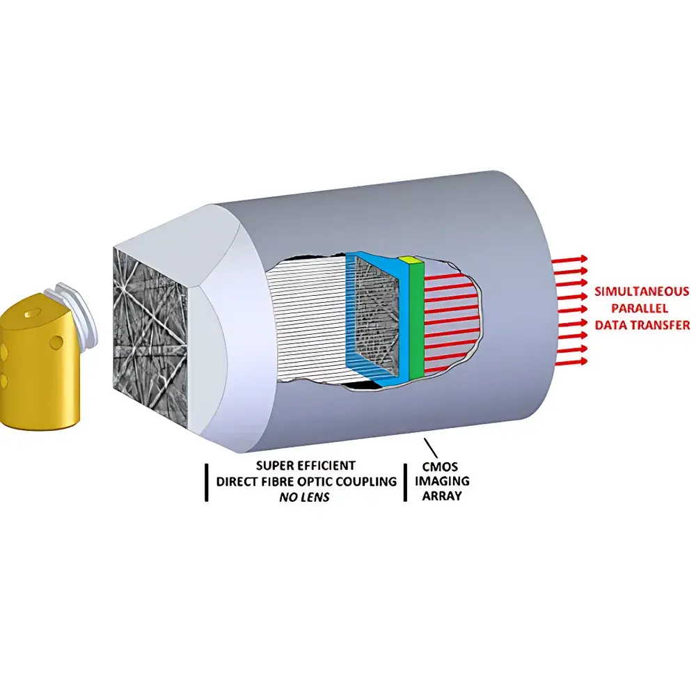
- Fiber-optic coupled scintillator design supporting high-speed acquisition at frame rates up to 1,000 fps (depending on binning and region of interest)
- Sub-pixel pattern distortion correction (<0.01° angular uncertainty) enabling quantitative strain mapping with <10⁻⁴ precision
- Motorized, software-controlled detector height adjustment accommodating samples ranging from bulk blocks to 10-µm-thick FIB lamellae
- Integrated beam alignment and screen positioning routines within AZtecCrystal software
Sample Compatibility & Compliance
NA-TKD supports a broad spectrum of crystalline and semi-crystalline specimens, including transmission electron microscopy (TEM) lift-outs, focused ion beam (FIB)-prepared cross-sections, epitaxial thin films, nanowires, and layered 2D materials. Its low-dose operation mode ensures minimal beam-induced damage during prolonged acquisition—critical for beam-sensitive oxides, polymers, and biological mineral composites. The system conforms to international standards for microstructural analysis: data acquisition protocols align with ASTM E112 (grain size measurement), ISO 14899-2 (EBSD methodology), and USP (crystallographic phase identification in pharmaceuticals). Full audit trail, user access control, and electronic signature support are embedded in AZtecCrystal software to meet GLP and FDA 21 CFR Part 11 requirements for regulated laboratories.
Software & Data Management
NA-TKD functionality is fully embedded within Oxford Instruments’ AZtecCrystal platform—a modular, scriptable, and validation-ready EBSD analysis suite. Real-time pattern indexing uses adaptive Hough transform algorithms with dynamic background subtraction and multi-phase confidence indexing. Strain analysis employs cross-correlation-based high-resolution EBSD (HR-EBSD) workflows, calibrated against NIST-traceable reference patterns. All raw pattern datasets are stored in HDF5 format with embedded metadata (beam energy, tilt angle, detector distance, stage coordinates), ensuring full FAIR (Findable, Accessible, Interoperable, Reusable) compliance. Batch processing pipelines support automated grain reconstruction, misorientation mapping, and texture component quantification across multi-region datasets.
Applications
- Quantitative dislocation density mapping in turbine superalloys via geometrically necessary dislocation (GND) analysis
- Crystallographic phase discrimination in multiphase battery cathode materials (e.g., NMC, LFP, solid electrolytes)
- Nanoscale orientation gradients in additively manufactured Ti-6Al-4V builds
- Strain partitioning at grain boundaries in irradiated nuclear fuel cladding alloys
- Orientation relationship determination in heteroepitaxial semiconductor stacks (e.g., GaN-on-SiC)
- In situ heating/cooling EBSD experiments requiring rapid pattern capture under thermal drift
FAQ
How does NA-TKD differ from conventional off-axis TKD?
NA-TKD relocates the phosphor screen to a position near the electron beam axis, reducing projection distortion and increasing solid-angle collection—yielding higher pattern contrast, improved angular resolution, and greater tolerance to beam drift.
Is NA-TKD compatible with non-Oxford SEMs?
Yes—provided the SEM chamber accommodates the Symmetry detector’s physical envelope and offers standard EDS/EBSD signal interfaces (e.g., TTL triggers, analog pattern output), NA-TKD can be retrofitted to FEI/Thermo Fisher, Zeiss, JEOL, and Hitachi platforms.
What minimum sample thickness is required for NA-TKD?
Optimal performance is achieved with electron-transparent regions ≤100 nm thick; however, reliable patterns have been acquired from samples as thick as 300 nm using 30 kV acceleration voltage and optimized detector geometry.
Does NA-TKD require specialized sample preparation?
Standard FIB lift-out or electropolishing remains sufficient; however, carbon contamination mitigation (e.g., low-kV cleaning, plasma etching) is strongly recommended prior to acquisition to preserve pattern fidelity during long-duration scans.
Can NA-TKD data be exported for third-party analysis?
Yes—AZtecCrystal exports calibrated Hough space parameters, indexed orientation matrices, and raw pattern arrays in open formats (HDF5, TIFF, CSV), fully interoperable with MTEX, EMsoft, and Python-based crystallography toolchains.


