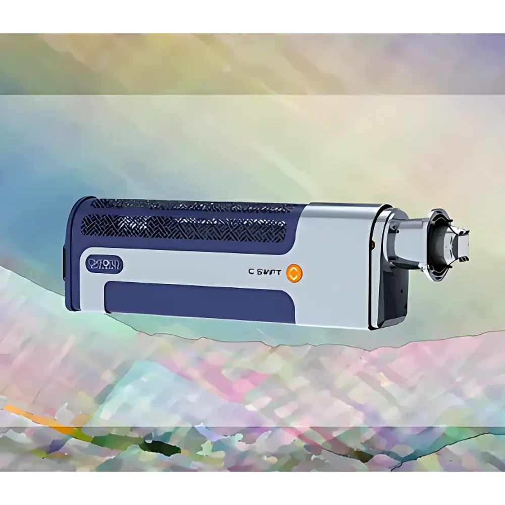
Oxford Instruments C-Swift EBSD Detector
| Brand | Oxford Instruments |
|---|---|
| Origin | United Kingdom |
| Model | C-Swift |
| CCD Camera Resolution | 1244 × 1024 |
| Maximum Frame Rate | 870 Hz |
| Spatial Resolution | 2 nm |
| Angular Resolution | < 0.05° |
Overview
The Oxford Instruments C-Swift EBSD Detector is a high-performance, CMOS-based electron backscatter diffraction (EBSD) system engineered for rapid, reliable, and quantitative microstructural characterization in scanning electron microscopes (SEM). Leveraging a purpose-built CMOS sensor architecture—derived from the proven Symmetry platform—the C-Swift delivers exceptional sensitivity, speed, and angular fidelity without compromising spatial resolution or signal integrity. Unlike legacy CCD-based detectors, the C-Swift operates on a fundamentally optimized optical-electronic pathway: its distortion-free lens system, high-efficiency phosphor screen, and low-noise readout electronics enable robust pattern acquisition across a wide range of beam conditions—including low kV (≤10 kV), low probe current (as low as 12 nA), and highly deformed or beam-sensitive materials. The detector is fully integrated into Oxford Instruments’ AZtec EBSD software suite, supporting real-time indexing, grain reconstruction, phase mapping, and strain analysis with traceable calibration and audit-ready metadata logging compliant with GLP and ISO/IEC 17025 workflows.
Key Features
- Ultra-high-speed acquisition: up to 1000 patterns per second (pps) at 156 × 128 pixel resolution—four times the effective pixel throughput of conventional CCD-based systems operating at comparable frame rates
- High-fidelity full-resolution mode: 622 × 512 pixel patterns at up to 250 pps, enabling precise phase identification, subgrain boundary detection, and lattice rotation quantification in multiphase or nanocrystalline samples
- Sub-0.05° angular resolution, achieved through aberration-corrected optics, thermal-stable mechanical design, and AZtec’s advanced Hough transform and confidence index algorithms
- Optimized phosphor screen with enhanced quantum efficiency for low-dose operation—enabling high-pattern-quality acquisition at beam currents down to 12 nA and accelerating voltage as low as 5 kV
- Integrated proximity sensor with automatic retraction mechanism ensures SEM chamber safety and eliminates risk of detector–specimen collision during stage navigation or tilt adjustment
- Flexible vacuum interface via bellows-mounted SEM flange, maintaining chamber integrity across variable-pressure and high-vacuum SEM configurations
- Five built-in front-end detectors for simultaneous acquisition of orientation contrast, atomic number (Z) contrast, and topographic signals—enabling correlative EBSD–EDS–BSE imaging without stage repositioning
Sample Compatibility & Compliance
The C-Swift detector supports broad material compatibility—from ductile metals (Al, Ti, Ni alloys) and ceramics (Al₂O₃, SiC) to geological specimens (quartz, olivine), polymers, and thin-film multilayers. Its low-beam-dose capability makes it suitable for beam-sensitive materials including battery cathode particles, MOFs, and biological mineral composites. All hardware and software components comply with CE marking requirements and are designed to meet essential provisions of the EU Machinery Directive 2006/42/EC. Data acquisition, processing, and reporting workflows align with ISO 13006 (ceramic tile microstructure), ASTM E112 (grain size measurement), ASTM E2627 (EBSD pattern quality assessment), and USP guidelines for analytical instrument qualification (AIQ). Optional 21 CFR Part 11-compliant audit trail and electronic signature modules are available for regulated pharmaceutical and medical device laboratories.
Software & Data Management
The C-Swift operates exclusively within Oxford Instruments’ AZtec EBSD platform—a modular, Windows-based application supporting automated calibration, dynamic background correction, multi-phase indexing, and machine-learning-assisted pattern classification. AZtec stores all raw pattern data, detector geometry parameters, beam conditions, and user annotations in a self-documenting HDF5 container format, ensuring full traceability and reproducibility. Batch processing pipelines support parallelized indexing across multi-core CPUs and GPU-accelerated pattern enhancement. Export options include standardized formats (TIFF, CSV, HDF5, OIM ASCII) compatible with third-party tools such as MTEX, Dream.3D, and ParaView. Data security protocols include role-based access control, encrypted local storage, and optional networked deployment with centralized license management and remote diagnostics.
Applications
- High-throughput grain structure mapping in additive manufacturing feedstock powders and build plates
- Crystallographic texture analysis of rolled aluminum sheets and cold-drawn copper wires
- Phase transformation kinetics studies in heat-treated steels and Ni-based superalloys
- Nanomechanical property correlation via kernel average misorientation (KAM) and geometrically necessary dislocation (GND) density mapping
- Interface characterization in solid-state battery electrodes (e.g., LiCoO₂/LiPON) and thermoelectric heterostructures
- Automated inclusion identification and classification in steel cleanliness assessment per ISO 4967
FAQ
What is the minimum beam current required for stable 1000 pps indexing?
A probe current of 12 nA at 15–20 kV is sufficient for consistent indexing at full speed on standard polished metal samples.
Can the C-Swift be retrofitted onto older SEM models?
Yes—the detector supports standard Ø100 mm or Ø120 mm SEM flanges and is compatible with FEI/Thermo Fisher, JEOL, Hitachi, and Zeiss SEM platforms manufactured after 2008.
Does the system support automated drift correction during long-duration mapping?
Yes—AZtec includes real-time stage drift compensation using fiducial tracking and adaptive pattern registration algorithms.
Is the 2 nm spatial resolution a measured value or theoretical specification?
The 2 nm figure refers to the effective pattern sharpness limit under optimal conditions (high-kV, high-current, ideal sample tilt and polish), validated against NIST-traceable grating standards.
How does the C-Swift handle dynamic background noise in low-signal environments?
AZtec implements adaptive dynamic background subtraction using rolling median filtering and pattern-specific noise modeling—preserving weak band contrast while suppressing stochastic noise.


