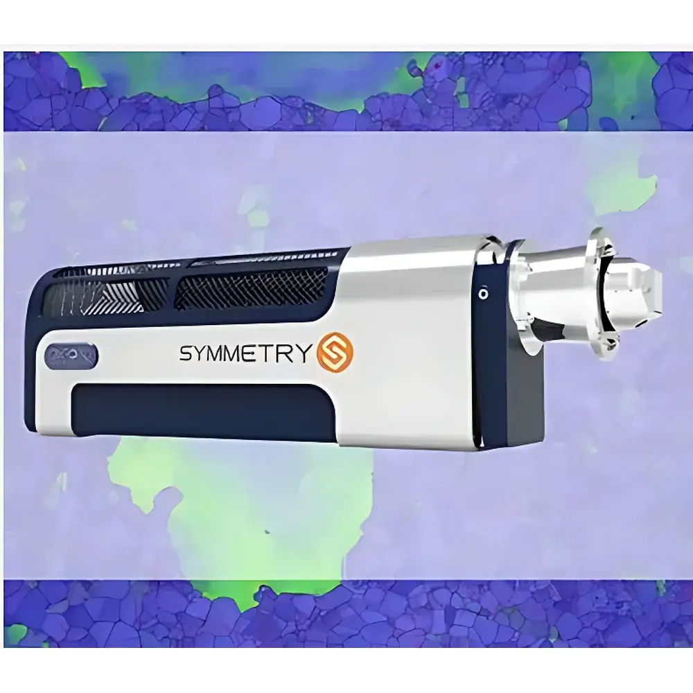
Oxford Instruments Symmetry S3 Electron Backscatter Diffraction (EBSD) Detector
| Brand | Oxford Instruments |
|---|---|
| Origin | United Kingdom |
| Model | Symmetry S3 |
| CCD Camera Resolution | 1244 × 1024 pixels |
| Maximum Acquisition Speed | 870 Hz (≥5700 patterns per second at 156 × 128 binning) |
| Spatial Resolution | 2 nm |
| Angular Resolution | <0.1° |
| Optical System | Lensless fiber-optic coupling |
| Sensor | Custom EBSD-optimized CMOS |
| Pattern Distortion | <1 pixel (sub-pixel guaranteed) |
| Sensitivity | up to 1000 pps/nA |
| Fluorescent Screen Travel Range | ±22 mm motorized vertical adjustment |
| Collision Protection | Patented proximity sensor system |
| Optional FSD | 5-diode front-scatter detector system |
Overview
The Oxford Instruments Symmetry S3 Electron Backscatter Diffraction (EBSD) Detector is a third-generation, high-performance EBSD acquisition system engineered for precision crystallographic characterization in scanning electron microscopy (SEM). Based on the well-established Symmetry platform, the S3 leverages advanced lensless fiber-optic coupling and a custom CMOS sensor optimized specifically for EBSD pattern fidelity, sensitivity, and temporal stability. It operates on the fundamental principle of detecting Kikuchi diffraction patterns generated by backscattered electrons from crystalline samples under controlled SEM beam conditions. These patterns are indexed in real time to determine crystal orientation, phase identity, grain boundaries, strain gradients, and lattice rotations—enabling quantitative microstructural analysis across metallurgy, geoscience, semiconductor development, additive manufacturing, and battery materials research. The S3 delivers robust performance across diverse beam energies (5–30 kV), working distances (10–25 mm), and sample tilt geometries (typically 70°), while maintaining sub-pixel pattern fidelity essential for high-resolution EBSD (HR-EBSD) and transmission Kikuchi diffraction (TKD).
Key Features
- Lensless fiber-optic coupling: Eliminates optical aberrations and chromatic distortion inherent in lens-based systems, ensuring consistent signal transmission and uniform quantum efficiency across the full field of view.
- Custom EBSD-optimized CMOS sensor: Delivers 1244 × 1024 pixel native resolution with >5700 patterns per second (pps) acquisition speed at 156 × 128 binned mode—enabling statistically robust grain size mapping in under 60 seconds per standard ISO 11839-compliant area.
- Motorized ±22 mm fluorescent screen travel: Enables precise geometric optimization for varied sample topographies, large-area stitching, and TKD-compatible configurations without manual intervention.
- Patented proximity sensor collision protection: Actively monitors detector position relative to the SEM stage and chamber components, automatically halting motion prior to physical contact—reducing unplanned downtime and safeguarding both detector and specimen.
- Software-controlled detector tilt: Allows dynamic adjustment of detector angle to maintain optimal pattern geometry across irregular or tilted samples, improving indexing confidence and angular reproducibility.
- Sub-pixel pattern distortion guarantee (<1 pixel): Validated through NIST-traceable calibration routines; critical for HR-EBSD applications requiring lattice rotation and elastic strain measurements with <0.01° real-time angular precision.
Sample Compatibility & Compliance
The Symmetry S3 is compatible with all major SEM platforms (FEI/Thermo Fisher, Zeiss, JEOL, Hitachi) via standardized vacuum interface flanges (CF-63 or CF-100) and integrated waveguide-compatible vacuum integrity. Its high sensitivity (up to 1000 pps/nA) supports low-dose analysis of beam-sensitive materials—including polymers, ceramics, and biological composites—without compromising pattern quality. For regulated environments, the system supports audit-trail-enabled data acquisition workflows compliant with GLP and GMP requirements when paired with AZtecCrystal software (v5.0+). While EBSD itself is not directly governed by FDA 21 CFR Part 11, Oxford Instruments provides documented validation protocols and electronic signature-ready reporting modules suitable for ISO 17025-accredited laboratories performing microstructural certification per ASTM E112 (grain size), ASTM E2627 (EBSD practice), and ISO 11839 (crystallographic texture).
Software & Data Management
Controlled exclusively through Oxford Instruments’ AZtecCrystal software suite, the Symmetry S3 integrates seamlessly with live indexing, automated phase identification, grain reconstruction, and misorientation mapping. The software implements real-time pattern center calibration (patent-pending high-precision mode), enabling angular accuracy better than 0.01° across variable working distances. All acquisition parameters—including camera mode selection (6 configurable modes), binning, exposure, and FSD diode activation—are stored as metadata within HDF5-formatted output files, ensuring full traceability and FAIR (Findable, Accessible, Interoperable, Reusable) data principles. Raw pattern datasets support batch reprocessing using machine-learning-enhanced indexing algorithms (e.g., dictionary-based matching, neural network classifiers) and export to common formats (TIFF, CSV, OIM ASCII) for third-party analysis in MATLAB, Python (EBSDtools, MTEX), or commercial FE simulation packages.
Applications
- High-resolution strain mapping: Quantitative measurement of elastic lattice distortions in turbine alloys, semiconductor heterostructures, and thin-film devices using HR-EBSD protocols.
- Transmission Kikuchi Diffraction (TKD): Enabled by fine-tuned screen positioning and ultra-low-dose capability—ideal for nanocrystalline metals, cross-sectional TEM lamellae, and ion-milled battery cathodes.
- Multimodal correlative imaging: Simultaneous acquisition of orientation contrast (via EBSD), topographic contrast (via secondary electrons), and Z-contrast (via optional upper FSD diodes) for comprehensive microstructure-property linkage.
- Additive manufacturing qualification: Rapid grain morphology, texture, and epitaxial growth analysis across build layers to assess process-induced anisotropy and recrystallization behavior.
- Geological phase mapping: Discrimination of polymorphs (e.g., quartz vs. coesite), deformation twins, and shear band networks in crustal rocks under low-kV SEM conditions.
FAQ
What vacuum interface standards does the Symmetry S3 support?
The detector is supplied with either CF-63 or CF-100 conflat flanges, fully compatible with standard SEM chamber ports and maintaining UHV integrity down to 1×10⁻⁷ mbar.
Is the Symmetry S3 compatible with older SEM models?
Yes—retrofit kits and mechanical adapters are available for legacy FEI Quanta, Zeiss EVO, and JEOL JSM series instruments; compatibility requires verification of chamber port location, clearance, and control signal availability.
Can the FSD system be used simultaneously with EBSD pattern acquisition?
Yes—the five-diode FSD operates independently and synchronously with the main EBSD camera, allowing concurrent acquisition of orientation, topography, and atomic number contrast without frame rate penalty.
Does Oxford Instruments provide application-specific validation documentation?
Yes—application notes, SOP templates, and IQ/OQ/PQ documentation packages are available upon request for regulated industries including aerospace, nuclear, and medical device manufacturing.
What maintenance is required for long-term stability?
No routine optical alignment or sensor recalibration is needed; the system features automatic self-check routines during startup, and only periodic cleaning of the phosphor screen (using nitrogen purge and lint-free wipes) is recommended per 6-month intervals.


