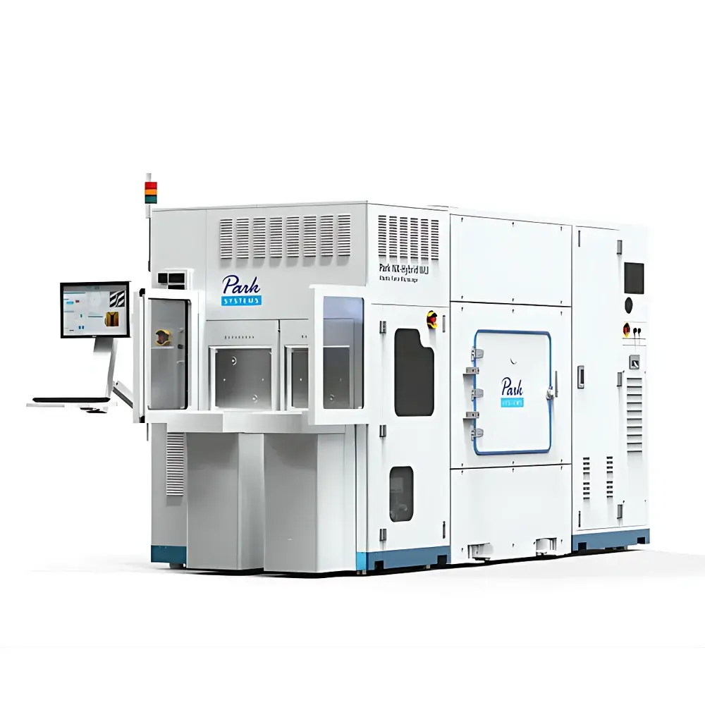
Park SYSTEMS NX-Hybrid WLI Atomic Force Microscope with Integrated White-Light Interferometry
| Brand | Park SYSTEMS |
|---|---|
| Origin | South Korea |
| Model | NX-Hybrid WLI |
| Wafer Compatibility | 300 mm (fully backward-compatible with 200 mm and smaller wafers) |
| Instrument Category | Optical Defect Inspection & Hybrid Metrology System |
| Primary Application | In-line semiconductor process monitoring and defect characterization |
| Core Technology Integration | Co-registered AFM + WLI on single platform |
| Measurement Capability | Sub-ångström vertical resolution (AFM), nanometer-level lateral resolution, µm-to-mm field-of-view (WLI) |
Overview
The Park SYSTEMS NX-Hybrid WLI is an industrial-grade, fully automated hybrid metrology platform that co-integrates atomic force microscopy (AFM) and white-light interferometry (WLI) within a single vacuum-compatible, cleanroom-ready instrument architecture. Engineered specifically for semiconductor front-end and back-end process control, it delivers traceable, high-reproducibility surface topography and defect metrology across the full wafer scale—from macro-scale uniformity assessment to localized sub-nanometer feature analysis. Unlike conventional sequential or offline metrology workflows, the NX-Hybrid WLI enables real-time, co-registered data acquisition: WLI rapidly scans large areas (up to 10 × 10 mm² per field) at throughput rates exceeding 30 wafers per hour (for standard defect screening protocols), while the integrated AFM module automatically navigates to user-defined regions-of-interest (ROIs) for quantitative, tip-based height measurements with sub-ångström vertical resolution and <1 nm lateral resolution. This dual-mode architecture eliminates stage repositioning errors, sample handling variability, and inter-instrument calibration drift—critical requirements for advanced node process development (≤3 nm logic, <10 nm DRAM) and heterogeneous integration metrology.
Key Features
- True co-registered AFM/WLI imaging: Single-stage, single-vacuum-chamber design ensures pixel-perfect spatial alignment between optical and probe-based datasets without manual registration or software interpolation.
- 300 mm full-wafer automation: Robust robotic handler compliant with SEMI E47.1 standards; supports SMIF/FOUP loading and integrated wafer mapping via built-in fiducial recognition.
- Sub-ångström height resolution (AFM): Achieved via low-noise, high-stiffness Z-sensor architecture and active vibration isolation (patented SmartScan™ feedback loop).
- High-throughput WLI mode: 5×–50× faster than conventional AFM-only inspection for blanket film uniformity, CMP residue detection, and step-height verification across >90% of die area.
- Cleanroom-certified mechanical design: ISO Class 5 compatible enclosure; non-outgassing materials; ESD-safe stage and probe handling system.
- Multi-modal defect correlation engine: Automatically links WLI-detected optical anomalies (e.g., haze, particles, scratches) to AFM-confirmed physical morphology (height, phase, adhesion) for root-cause classification.
Sample Compatibility & Compliance
The NX-Hybrid WLI accommodates bare silicon, SiO₂, SiN, low-k dielectrics, metal stacks (Cu, Co, Ru), and emerging 2D materials (MoS₂, h-BN) without requiring conductive coating. Its non-contact WLI mode enables rapid inspection of transparent or fragile films (e.g., photoresists, spin-on-glass) where traditional AFM tip contact may induce artifacts. The system meets SEMI S2/S8 safety specifications, complies with ISO/IEC 17025 guidelines for metrological traceability, and supports audit-ready documentation per FDA 21 CFR Part 11 and ISO 9001 quality management frameworks. All measurement routines—including step-height calibration, tip wear monitoring, and WLI fringe contrast optimization—are validated against NIST-traceable step-height standards (e.g., VLSI Standards SRM 2160).
Software & Data Management
XEI™ 7.0 software provides unified control, analysis, and reporting across both modalities. It features automated recipe-driven workflows for process qualification (PQ), equipment qualification (EQ), and statistical process control (SPC) charting. Raw data is stored in vendor-neutral HDF5 format with embedded metadata (timestamp, operator ID, environmental conditions, calibration status). Audit trails record all parameter modifications, image exports, and report generations—enabling full GLP/GMP compliance. Integration with factory MES via SECS/GEM protocol allows direct upload of pass/fail metrics (e.g., RMS roughness, defect density, edge profile slope) into yield management databases.
Applications
- Front-end process control: Gate oxide thickness uniformity, fin height/cd variation, STI trench depth, EUV resist line-edge roughness (LER), and spacer CD metrology.
- Back-end and advanced packaging: Cu pillar height, under-bump metallization (UBM) planarity, TSV sidewall roughness, and microbump coplanarity assessment.
- Defect root-cause analysis: Distinguishing particle-induced topographic perturbations from intrinsic film delamination or stress-induced buckling via correlated phase/height/deflection signals.
- Materials R&D: Quantitative nanomechanical mapping (modulus, adhesion) of novel low-k dielectrics and high-mobility channel materials using AFM-based force spectroscopy modules.
- Process qualification: Full-wafer uniformity mapping for ALD/CVD film thickness, CMP removal rate, and etch selectivity validation.
FAQ
Does the NX-Hybrid WLI require separate calibration for AFM and WLI modes?
No. The system employs a monolithic metrology frame with shared encoder feedback and laser-interferometric position referencing, ensuring inherent calibration consistency between both modalities without user intervention.
Can it measure transparent thin films on silicon substrates?
Yes. WLI operates effectively on optically transparent layers (e.g., SiO₂, SiN, polymers) up to ~10 µm thick. For sub-surface interface analysis, AFM phase imaging complements WLI by detecting material contrast independent of optical reflectivity.
Is the system compatible with existing fab automation infrastructure?
Yes. It supports standard SEMI E30/E40/E54 communication protocols, integrates with AMHS via SECS/GEM, and provides OPC UA server capability for Industry 4.0 data federation.
What is the typical maintenance interval for the AFM probe exchange mechanism?
Under continuous 24/7 operation in Class 5 cleanroom environments, the automated probe loader is rated for ≥50,000 cycles before scheduled preventive maintenance, per Park SYSTEMS’ Field Service Bulletin FS-2023-08.
How does the system handle thermal drift during long-duration WLI scans?
The WLI module incorporates real-time thermal compensation using dual-point platinum resistance thermometers (PRTs) embedded in the optical path and stage assembly, limiting Z-drift to <0.15 nm/°C over 2-hour acquisitions.


