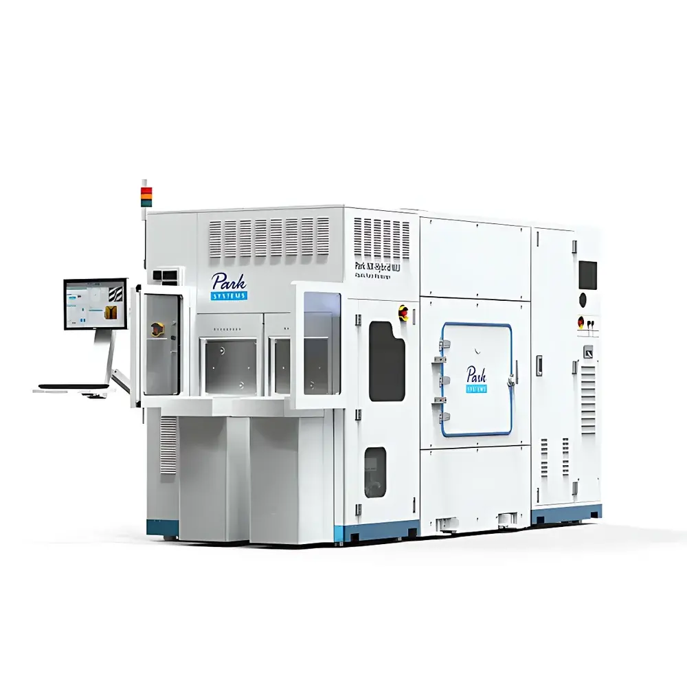
Park SYSTEMS NX-Hybrid WLI White Light Interferometry–Atomic Force Microscopy Hybrid Metrology System
| Brand | Park SYSTEMS |
|---|---|
| Origin | South Korea |
| Model | NX-Hybrid WLI |
| Primary Technology | Integrated White Light Interferometry (WLI) and Atomic Force Microscopy (AFM) |
| Optical Modes | WLI & Phase-Shifting Interferometry (PSI) |
| Objective Lenses | 2.5×, 10×, 20×, 50×, 100× (motorized turret) |
| Interferometric Objective Type | Mirau |
| Measurement Principle | Coherence scanning interferometry with sub-nanometer vertical resolution |
| Application Domain | Semiconductor front-end & back-end process control, advanced packaging metrology, wafer-level defect review, CMP characterization, GLP/GMP-compliant R&D and inline QA |
Overview
The Park SYSTEMS NX-Hybrid WLI is a purpose-engineered hybrid metrology platform that co-integrates white light interferometry (WLI) and atomic force microscopy (AFM) within a single, unified instrument architecture. Designed specifically for semiconductor process development and high-precision manufacturing, it bridges the performance gap between optical and scanning probe techniques—enabling quantitative surface topography analysis across spatial scales ranging from millimeters to nanometers. Unlike conventional standalone systems, the NX-Hybrid WLI performs simultaneous or sequential WLI and AFM measurements on identical sample locations without repositioning, eliminating registration error and ensuring traceable correlation between macro-scale morphology and nanoscale feature fidelity. Its core measurement principle relies on coherence scanning interferometry: a Mirau-type objective generates interference fringes as the reference mirror scans axially; the envelope of fringe contrast is tracked pixel-wise to reconstruct surface height with sub-nanometer vertical repeatability. When combined with Park’s high-stability AFM stage and low-noise piezoelectric scanner, the system delivers metrologically rigorous data compliant with ISO 25178 (surface texture), ASTM E2949 (CMP surface uniformity), and SEMI standards for wafer inspection.
Key Features
- Integrated dual-mode optical head supporting both white light interferometry (WLI) and phase-shifting interferometry (PSI) via motorized filter changer—optimized for high-speed large-area survey (WLI) and ultra-high-resolution step-height quantification (PSI).
- Motorized objective turret accommodating five magnifications (2.5×, 10×, 20×, 50×, 100×), enabling seamless transition between macro-defect screening and micro-feature verification.
- Co-registered AFM–WLI coordinate system with <100 nm lateral registration accuracy—critical for defect navigation, hotspot localization, and correlative metrology workflows.
- High-stability closed-loop AFM scanner with sub-angstrom vertical resolution and active thermal drift compensation—validated per ISO/IEC 17025 calibration protocols.
- Automated stage with 100 mm × 100 mm travel range and ≤ ±0.5 µm positioning repeatability—suitable for full-wafer mapping and multi-site process monitoring.
- Real-time WLI-based defect detection algorithm capable of identifying pattern anomalies, residues, and topology deviations at throughput rates exceeding 10 wafers/hour (200 mm), with configurable sensitivity thresholds aligned to ITRS roadmap requirements.
Sample Compatibility & Compliance
The NX-Hybrid WLI supports bare silicon, SOI, compound semiconductors (GaAs, SiC, GaN), low-k dielectrics, metal interconnects, TSVs, redistribution layers (RDL), and 2.5D/3D packaging substrates—including fan-out wafer-level packages (FOWLP) and silicon interposers. It accommodates standard wafer formats (100 mm to 300 mm) with optional vacuum chuck or edge-grip handling. All measurement routines are fully compatible with ISO 9001 quality management systems and support audit-ready documentation per FDA 21 CFR Part 11 when deployed in regulated environments. Data integrity is ensured through hardware-enforced timestamping, user-access controls, and electronic signature capability. The system meets SEMI S2/S8 safety requirements and operates within Class 100 cleanroom specifications.
Software & Data Management
XEI software v5.0 provides unified control of both WLI and AFM modules, featuring scriptable automation (Python API), batch processing pipelines, and hierarchical data storage compliant with ASAM ODS standards. Defect maps generated by WLI are directly overlaid onto AFM coordinate grids, enabling one-click navigation to review sites. Statistical process control (SPC) dashboards integrate with factory MES systems via SECS/GEM interface. Raw interferograms and AFM force curves are stored in HDF5 format with embedded metadata (instrument configuration, environmental logs, calibration history). Software validation packages—including IQ/OQ documentation and test scripts—are available for GxP-regulated laboratories.
Applications
- Chemical-mechanical polishing (CMP) process monitoring: Quantitative evaluation of dishing, erosion, and within-wafer non-uniformity (WIWNU) across full-die and wafer-scale regions.
- Advanced packaging metrology: Warpage mapping of thin wafers, bump height uniformity assessment, and underfill void detection in 2.5D/3D IC stacks.
- Mask and reticle inspection support: High-throughput identification of pellicle defects, chrome pitting, and quartz substrate scratches followed by AFM-based root-cause analysis.
- Failure analysis (FA) workflow acceleration: Rapid localization of electrical failure sites using WLI-generated topographic signatures, followed by nanoscale cross-sectional imaging via AFM nano-scratching or conductive-AFM.
- Surface roughness certification: Sub-Ångström Sa/Sq measurement on epitaxial layers and ALD films—traceable to NIST SRM 2160 reference standards.
FAQ
How does the NX-Hybrid WLI ensure measurement traceability between WLI and AFM datasets?
Through a mechanically fixed, thermally stable coordinate frame and laser-interferometric stage calibration—verified during factory acceptance testing and documented per ISO/IEC 17025.
Can the system perform automated defect review without manual intervention?
Yes: WLI-based defect detection triggers programmed AFM acquisition at specified coordinates, with configurable pass/fail criteria and auto-report generation.
Is PSI mode required for all high-precision measurements?
No: PSI provides superior step-height accuracy (<0.1 nm) on near-perfectly flat, coherent surfaces; WLI remains preferred for rough, tilted, or multi-material structures where fringe visibility is limited.
What level of training is required to operate the system in production environments?
Operators require 2 days of certified training covering SOP execution, preventive maintenance, and basic data interpretation; engineers receive additional 3-day advanced metrology curriculum including uncertainty budgeting and SPC integration.
Does the system support remote diagnostics and firmware updates?
Yes: Secure TLS-encrypted remote access is available via Park’s CloudConnect service, with version-controlled firmware deployment and real-time health monitoring.


