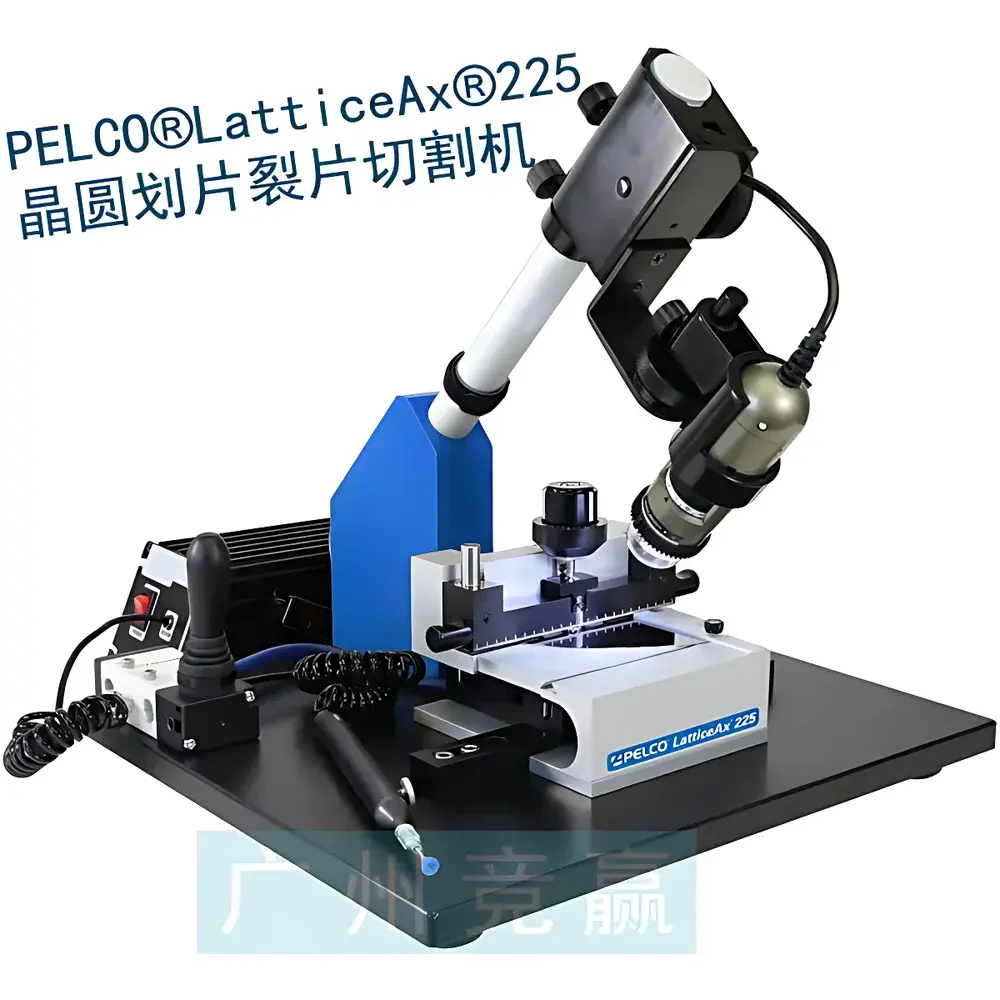
PELCO LatticeAx 225 Precision Manual Wafer Scribing and Cleaving System
| Brand | Ted Pella |
|---|---|
| Origin | USA |
| Manufacturer Type | Authorized Distributor |
| Product Origin | Imported |
| Model | LatticeAx 225 |
| Maximum Scribe Line Speed | 600 mm/min |
| Application Scope | Semiconductor Wafers, MEMS, Optoelectronics, and Thin-Film Devices |
| Positioning Accuracy | ±20 µm |
| Scribe Impression Length | <1 mm |
| Impression Width | ~10 µm |
| Imaging System | USB 2.0 Digital Microscope with Polarizing Filter and Real-Time Capture Software |
| Vacuum Fixation | Pneumatically Actuated Valve-Controlled Pump |
| Sample Compatibility | Si, SiC, GaAs, Sapphire, Glass, Quartz, and Thin-Film Substrates (Ø50–300 mm, Thickness 100–1000 µm) |
Overview
The PELCO® LatticeAx® 225 is a precision manual scribing and cleaving system engineered for controlled, crystallographic separation of semiconductor wafers and brittle substrates without mechanical kerf loss or thermal damage. Unlike conventional dicing saws that rely on abrasive blade cutting—introducing debris, chipping, and subsurface damage—the LatticeAx 225 implements a deterministic “cleavage-based scribing” methodology grounded in anisotropic fracture mechanics. It utilizes a diamond-tipped scribe stylus to induce a sub-micron-width, sub-1 mm-length mechanical impression along a selected crystallographic plane. This localized stress perturbation initiates controlled cleavage propagation when subjected to a calibrated bending moment, yielding atomically defined fracture surfaces aligned with low-energy lattice planes. The system is purpose-built for R&D laboratories, failure analysis centers, and pilot-line packaging facilities where preservation of device integrity, minimal material loss, and high positional fidelity are non-negotiable requirements.
Key Features
- ±20 µm mechanical positioning accuracy enabled by a rigid, vibration-damped granite base and micrometer-adjustable XYZ translation stage
- Dual-mode imaging interface: integrated USB 2.0 digital microscope with polarizing optics, fine-focus micromanipulator, and real-time image acquisition software for sub-pixel scribe line registration
- Cleavage-specific scribing protocol: eliminates traditional scoring-and-breaking ambiguity by coupling precise impression geometry (<1 mm length, ~10 µm width) with crystallographically guided fracture initiation
- Pneumatic vacuum chuck with solenoid-controlled valve ensures repeatable, non-marring sample fixation across wafer diameters from 50 mm to 300 mm and thicknesses from 100 µm to 1 mm
- Tool-free stylus exchange system supporting interchangeable diamond tips (standard 30° included; optional 15°/45° angles for specific cleavage orientations)
- Compliance-ready design: fully traceable mechanical calibration points, documented alignment procedures, and audit-log-capable imaging metadata export (TIFF + XML sidecar)
Sample Compatibility & Compliance
The LatticeAx 225 accommodates a broad spectrum of single-crystal and polycrystalline substrates relevant to compound semiconductor fabrication, MEMS prototyping, and optoelectronic packaging. Validated materials include silicon (100), silicon carbide (4H-SiC), gallium arsenide (100), sapphire (c-plane), fused silica, borosilicate glass, and thin-film-coated wafers with dielectric or metallic layers up to 5 µm thick. All scribe parameters—including impression depth, lateral force, and cleavage loading profile—are adjustable within ISO 9001-aligned operating procedures. The system supports GLP-compliant documentation workflows via timestamped image archives, operator ID tagging, and configurable report templates compatible with LIMS integration. While not a production-line tool, its output meets ASTM F1782-22 (Standard Practice for Cleaving Brittle Materials) and aligns with JEDEC JESD22-A113 (Mechanical Shock Testing) sample preparation guidelines.
Software & Data Management
The included imaging software suite operates on Windows 10/11 (64-bit) and provides real-time overlay of crosshair-guided scribe coordinates onto live microscope feeds. It supports hardware-triggered frame capture synchronized with scribe actuation, automatic contrast optimization for low-reflectivity substrates (e.g., SiC, GaN), and batch export of annotated TIFF sequences with embedded EXIF metadata (pixel scale, magnification, timestamp, operator ID). Raw image data retains full 12-bit dynamic range for post-acquisition quantitative analysis. No cloud dependency or subscription licensing is required; all processing occurs locally. Audit trail functionality complies with FDA 21 CFR Part 11 requirements when paired with institutional electronic signature protocols and validated IT infrastructure.
Applications
- Rapid prototyping of photonic integrated circuits (PICs) requiring mirror-smooth facet cleavage for laser cavity formation
- Preparation of TEM lamellae from device-grade wafers without ion-beam damage or redeposition artifacts
- Controlled singulation of MEMS accelerometers and gyroscopes to preserve hermetic seal integrity
- Sectioning of perovskite solar cell stacks for cross-sectional SEM/EDS analysis with minimized interfacial delamination
- Low-yield qualification of GaN-on-Si HEMT wafers prior to full-scale dicing, reducing scrap cost
- Failure analysis of cracked die edges in high-reliability aerospace ICs using crystallographically matched fracture surface reconstruction
FAQ
Does the LatticeAx 225 require consumables beyond the diamond stylus?
No. The system uses no coolant, lubricants, or disposable blades. Diamond stylus lifetime exceeds 500 cleaves per tip under standard Si(100) conditions; replacement kits include calibration verification certificates.
Can it process wafers with backside metallization or temporary bonding tapes?
Yes—provided the tape modulus allows sufficient bending compliance during cleavage. Recommended tape types include UV-curable acrylics (e.g., Nitto DAF series) and thermoplastic films with Tg < 80°C.
Is training provided with purchase?
Ted Pella delivers a 4-hour remote application workshop covering substrate selection, crystallographic indexing, impression parameter optimization, and cleavage force calibration—recorded and available for institutional retraining.
How does it compare to laser stealth dicing for small-batch R&D?
LatticeAx 225 offers superior edge quality (Ra < 5 nm vs. typical 20–50 nm for laser), zero heat-affected zone, and no need for post-process cleaning. It lacks throughput scalability but excels in ultra-low-volume, high-fidelity applications where metrology-grade cleavage is mandatory.
What maintenance schedule is recommended?
Biannual verification of stage orthogonality (using NIST-traceable gauge blocks) and annual microscope resolution validation (via USAF 1951 target) constitute the full preventive maintenance protocol. No internal calibration is user-serviceable.


