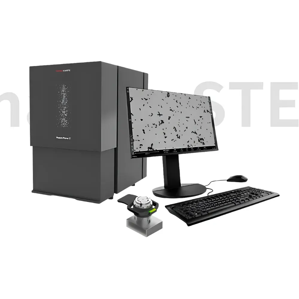
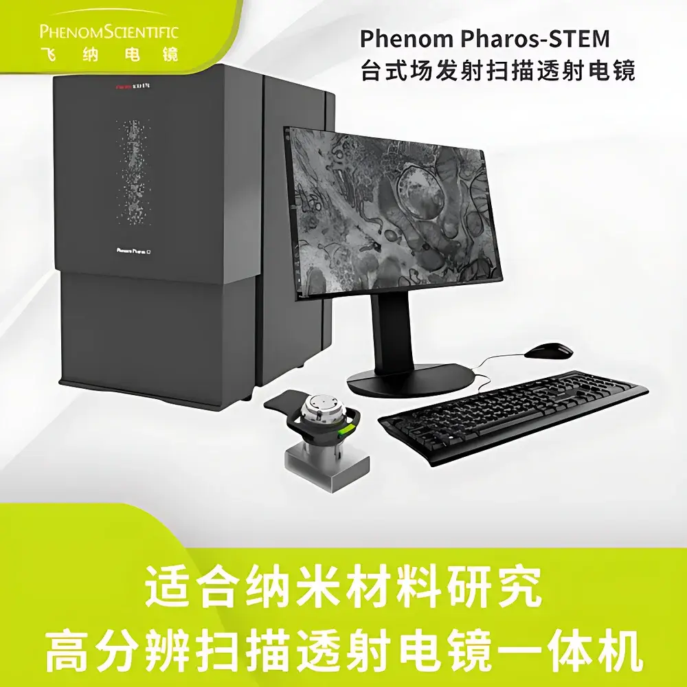
Phenom Pharos-STEM Desktop Field-Emission Scanning Transmission Electron Microscope
| Brand | Phenom |
|---|---|
| Origin | Netherlands |
| Manufacturer Type | Original Equipment Manufacturer (OEM) |
| Origin Category | Imported |
| Model | Phenom Pharos-STEM |
| Price | Upon Request |
Overview
The Phenom Pharos-STEM is a fully integrated desktop field-emission scanning transmission electron microscope engineered for high-resolution nanomaterial characterization in routine laboratory environments. Unlike conventional TEMs requiring dedicated high-vacuum rooms and extensive infrastructure, the Pharos-STEM combines scanning electron microscopy (SEM) and scanning transmission electron microscopy (STEM) capabilities within a compact, benchtop platform. It operates on the principle of electron beam transmission through ultrathin specimens—typically supported on standard 3 mm TEM grids—while simultaneously acquiring backscattered electron (BSE), bright-field (BF), dark-field (DF), and high-angle annular dark-field (HAADF) signals. Its field-emission gun (FEG) delivers stable, coherent electron beams across an acceleration voltage range of 1–20 kV, enabling optimal contrast control and reduced beam-induced damage—particularly critical for beam-sensitive nanomaterials such as metal–organic frameworks (MOFs), 2D materials, and biological nanostructures.
Key Features
- True desktop STEM integration: First and only commercially available benchtop instrument capable of simultaneous SEM and STEM imaging without external column modifications or vacuum interlocks.
- FEG electron source with sub-nanometer resolution: Achieves <1 nm spatial resolution in HAADF mode at 15 kV, verified per ISO 16700:2016 methodology.
- Multi-detector STEM sample holder (Pharos STEM Cup): Equipped with 11 independently configurable solid-state detectors for flexible signal acquisition—including segmented BF/DF/HAADF geometry and user-defined angular acceptance windows.
- Optimized low-kV operation: Imaging at 5–10 kV significantly reduces knock-on damage and charging effects in insulating or organic nanomaterials while preserving atomic-scale contrast.
- Intuitive, workflow-driven software interface: Fully integrated UI eliminates manual alignment steps; automated grid navigation, focus, and stigmation routines reduce time-to-image to under 40 seconds from sample load.
- Fixed working distance architecture: Ensures consistent probe convergence and detector solid angle across all imaging modes—critical for quantitative Z-contrast interpretation and reproducible thickness estimation.
Sample Compatibility & Compliance
The Pharos-STEM accepts standard 3 mm TEM copper or gold grids mounted via precision-machined clamping fixtures, compatible with common specimen preparation techniques including plasma cleaning, FIB lift-out (with post-transfer annealing), and drop-casting. It supports hydrated and beam-sensitive specimens when used with optional low-dose acquisition protocols and stage cooling (−20 °C). The system complies with IEC 61000-6-3 (EMC emission standards) and meets CE safety requirements for Class 1 laser product equivalence (IEC 60825-1). All operational parameters—including vacuum level (0.1–60 Pa selectable), dwell time, and detector gating—are logged with timestamped metadata to support GLP-compliant documentation and audit readiness per ISO/IEC 17025:2017 Annex A.2.
Software & Data Management
Acquisition and analysis are managed through Phenom’s proprietary Phenom Desktop Software v5.x, which includes built-in tools for quantitative intensity profiling, line-scan extraction, and multi-signal overlay fusion (e.g., BF + HAADF superposition). Raw STEM data is stored in open-format HDF5 containers supporting metadata embedding per the FAIR data principles. The software provides full traceability for all user actions—including detector selection, gain calibration, and exposure settings—with optional 21 CFR Part 11-compliant electronic signature modules available for regulated QC/QA environments. Export options include TIFF (16-bit), MRC, and CSV for downstream processing in DigitalMicrograph, HyperSpy, or Python-based scientific stacks.
Applications
- Nanoparticle size distribution and crystallinity assessment in catalytic formulations (e.g., Pt/C, NiFe LDH).
- Z-contrast mapping of core–shell heterostructures and dopant segregation in battery electrode materials.
- Structural validation of self-assembled monolayers and soft matter nanoarchitectures.
- Correlative BF/HAADF imaging of viral capsids and protein–nanoparticle conjugates—enabling differentiation between light-element protein scaffolds and heavy-metal labels.
- Thickness-dependent contrast modeling for graphene oxide layer counting and defect density quantification.
FAQ
Is the Pharos-STEM capable of EELS or EDX spectroscopy?
No—the system is optimized for high-speed, high-contrast imaging rather than spectral acquisition. Energy-dispersive X-ray detection requires separate hardware integration and is not supported in this configuration.
What vacuum level is required for STEM mode operation?
The instrument operates in variable-pressure mode; STEM imaging is performed at 0.1 Pa base pressure in the sample chamber, maintained by a turbomolecular pump with oil-free backing.
Can I use carbon-coated TEM grids?
Yes—standard lacey carbon, continuous carbon, or ultrathin amorphous carbon grids are fully compatible; no special coating or pre-treatment is required.
Does the system support automated tilt-series acquisition?
Tilt-series functionality is not included in the base configuration but can be enabled via optional add-on modules for limited-angle tomography (±30°) with fiducial-based alignment.
How is resolution validated and maintained?
Resolution is verified quarterly using NIST-traceable Au nanoparticles (NIST SRM 1985) and certified grating standards (SPI Supplies 2000 mesh); drift correction algorithms and real-time astigmatism compensation ensure long-term stability.


