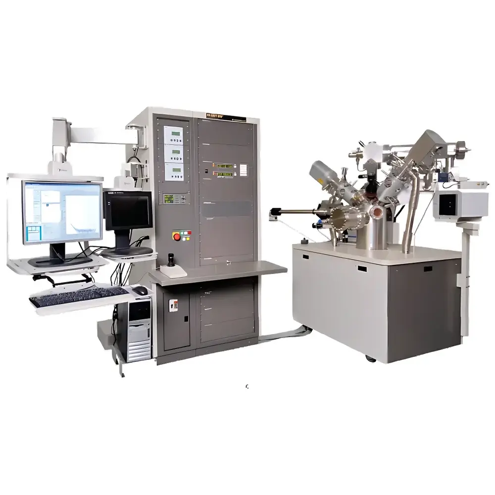
PHI ADEPT-1010 Dynamic Secondary Ion Mass Spectrometer
| Brand | ULVAC-PHI |
|---|---|
| Origin | Japan |
| Model | PHI ADEPT-1010 |
| Instrument Type | Quadrupole |
| Primary Beam Energy Range | 0.25–11 keV |
| Mass Range | 1–340 amu |
| Distribution Status | Authorized Distributor (Imported) |
Overview
The PHI ADEPT-1010 Dynamic Secondary Ion Mass Spectrometer (SIMS) is a high-performance, quadrupole-based surface analysis instrument engineered for quantitative depth profiling and molecular surface characterization of solid materials. Operating on the principle of sputter-initiated secondary ion emission, the system utilizes a focused primary ion beam—typically O+, Cs+, or Ga+—to bombard the sample surface, ejecting secondary ions that retain elemental, isotopic, and limited molecular information. These ejected ions are mass-analyzed with high transmission efficiency by a robust quadrupole mass filter and detected using a discrete-dynode electron multiplier. Designed for dynamic SIMS mode (high primary beam current, continuous sputtering), the ADEPT-1010 delivers excellent sensitivity for trace element detection (sub-ppm level in many matrices) and high-depth-resolution profiling—particularly critical for semiconductor metrology, thin-film stack analysis, and dopant distribution mapping in advanced microelectronics.
Key Features
- Quadrupole mass analyzer optimized for dynamic SIMS operation, offering stable mass calibration and repeatable peak shape across the full 1–340 amu range
- Variable-energy primary ion gun supporting 0.25–11 keV acceleration, enabling controlled sputter yield modulation and matrix effect mitigation
- Dual-beam capability (optional): simultaneous or alternating primary ion sources (e.g., O+/Cs+) for enhanced ionization efficiency across electropositive and electronegative elements
- High-vacuum UHV-compatible chamber (<1×10⁻⁹ Torr base pressure) with cryo-pumped sample stage to minimize hydrocarbon contamination and preserve surface integrity
- Integrated beam rastering and stage positioning with sub-micron reproducibility, supporting automated multi-point analysis and lateral imaging (up to 200 µm × 200 µm field)
- Modular design compliant with ISO 14644-1 Class 5 cleanroom integration requirements; compatible with load-lock transfer for air-sensitive samples
Sample Compatibility & Compliance
The PHI ADEPT-1010 accommodates conductive and semiconductive solid specimens up to 25 mm in diameter and 10 mm in thickness—including Si wafers, III–V compounds, metal oxides, perovskites, and layered 2D materials. Non-conductive samples may be analyzed with charge compensation via low-energy electron flood gun. All operational parameters—including beam energy, dwell time, and sputter rate—are logged with timestamp and user ID to support GLP/GMP-aligned workflows. The system meets essential electromagnetic compatibility (EMC) requirements per IEC 61326-1 and conforms to vacuum safety standards per ISO 27874. While not FDA-cleared as a medical device, its data output structure supports audit-trail generation for 21 CFR Part 11-compliant environments when paired with validated laboratory information management systems (LIMS).
Software & Data Management
Control and data acquisition are managed through PHI’s proprietary MultiPak™ software suite, which provides real-time spectral display, depth-scale calibration (via SRM reference standards), and batch processing of depth profiles. Raw data files (.raw) store full metadata—including instrument configuration, vacuum status, and beam alignment history—in ASCII-compatible format for third-party spectral deconvolution (e.g., PeakFit, IGOR Pro) or statistical process control (SPC) integration. Software supports ASTM E1527-20 compliant reporting templates for semiconductor industry depth profiling certification. Automated calibration routines include mass axis verification using known peaks (e.g., 12C+, 16O+, 28Si+) and intensity normalization against internal reference signals.
Applications
- Quantitative dopant depth profiling in CMOS gate stacks and FinFET channel regions
- Interface chemistry analysis of high-k dielectric/metal gate stacks (e.g., HfO2/TiN)
- Trace contaminant mapping (e.g., Na, K, Cl) in photovoltaic absorber layers (CIGS, perovskite)
- Isotopic ratio measurement for diffusion studies (e.g., 18O tracer in oxide growth kinetics)
- Failure analysis of interconnect voids and barrier layer integrity in advanced packaging
- Surface segregation quantification in catalyst nanoparticles and battery electrode coatings
FAQ
What vacuum level is required for optimal ADEPT-1010 performance?
The instrument requires a base pressure ≤1×10⁻⁹ Torr, achieved via turbomolecular pumping supplemented by cryogenic trapping. Residual gas analysis confirms H2O and CO partial pressures remain below 1×10⁻¹¹ Torr during analysis.
Can the ADEPT-1010 perform static SIMS measurements?
No—the ADEPT-1010 is specifically configured for dynamic SIMS operation. Static SIMS (low-dose, surface-sensitive mode) requires ultra-low beam currents (<10−12 A) and time-of-flight detection, which are not supported by this quadrupole platform.
Is depth resolution affected by primary beam energy selection?
Yes. Lower beam energies (e.g., 0.25–1 keV) generally improve depth resolution in shallow profiles (<5 nm), while higher energies (≥5 keV) increase sputter rate at the expense of interface broadening due to increased ion implantation and mixing.
How is quantification performed without matrix-matched standards?
Relative sensitivity factors (RSFs) derived from certified reference materials (e.g., NIST SRM 2137 for Si-based systems) are applied. For non-standard matrices, RSF interpolation using elemental periodic trends and published literature values is supported within MultiPak™.
Does the system support automated wafer handling?
Yes—optional robotic load-lock integration enables unattended analysis of up to 25 standard 100–300 mm wafers per run, with integrated pattern recognition for die-level targeting.
")
")