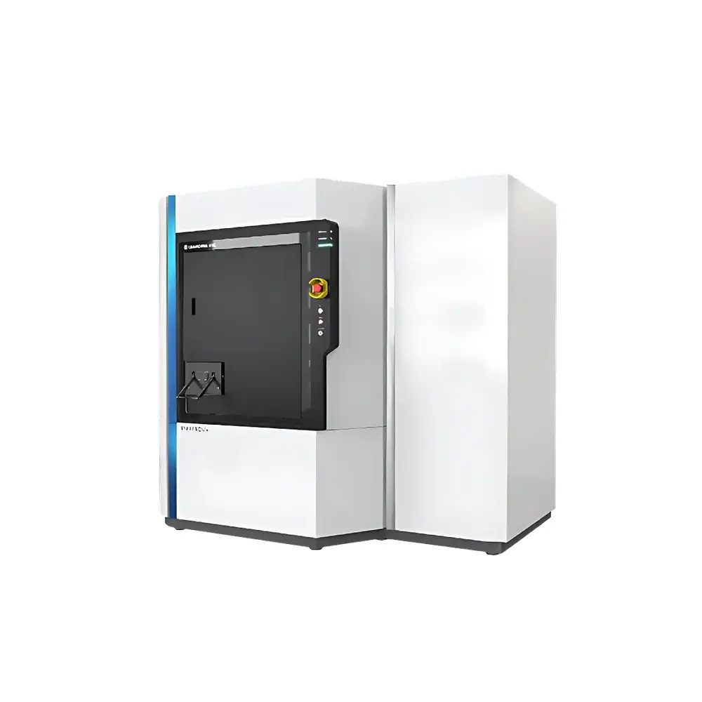
PHI Genesis 500 X-Ray Photoelectron Spectrometer
| Brand | PHI |
|---|---|
| Origin | Japan |
| Model | Genesis 500 |
| Type | Fully Automated Scanning Focused XPS System |
| Sample Stage | Motorized 3-Position Carousel (80 mm × 80 mm trays) |
| Microprobe Spot Size | ≤ 5 µm |
| Depth Profiling | Integrated High-Performance Ar⁺ Ion Gun + Dual-Beam Charge Neutralization |
| Optional Techniques | UPS, LEIPS, REELS, AES, HAXPES, GCIB Sputtering |
| Software Platform | PHI SmartSoft Suite with GLP/GMP-Compliant Audit Trail & 21 CFR Part 11 Support |
| Compliance | ASTM E1521, ISO 18118, ISO 21365, USP <1057>, IEC 62304 |
Overview
The PHI Genesis 500 is a next-generation, fully automated scanning focused X-ray photoelectron spectrometer engineered for high-precision surface and interface chemical state analysis. Based on the core principle of photoemission spectroscopy—where monochromatic Al Kα (1486.6 eV) or optional Mg Kα X-rays eject photoelectrons from topmost atomic layers—the instrument delivers quantitative elemental composition, chemical bonding information (oxidation states, functional groups), and depth-resolved electronic structure with sub-nanometer surface sensitivity. Its integrated scanning X-ray source enables both large-area survey mapping (up to 80 mm × 80 mm per sample tray) and microscale spatial resolution (≤ 5 µm beam spot), making it uniquely suited for heterogeneous, multi-layered, and insulating materials common in advanced energy and microelectronics research.
Key Features
- Fully motorized 3-position sample carousel with automatic load-lock transfer, enabling unattended sequential analysis of up to three pre-loaded trays without breaking vacuum.
- Scanning monochromated X-ray source delivering ≤ 5 µm focused beam for high-spatial-resolution XPS mapping, secondary electron imaging (SXI), and correlated microanalysis.
- High-transmission hemispherical analyzer with 180° double-pass optics and multi-channel detection, optimized for signal-to-noise ratio across wide kinetic energy ranges (0–1500 eV).
- Integrated high-stability Ar⁺ ion gun (0.1–5 kV, beam diameter adjustable to ≤ 100 µm) with dual-beam low-energy electron and Ar⁺ neutralization for stable charge compensation on insulators during depth profiling.
- Modular accessory architecture supporting simultaneous or sequential operation of UPS (ultraviolet photoelectron spectroscopy), LEIPS (low-energy inverse photoemission spectroscopy), REELS (reflected electron energy loss spectroscopy), AES (Auger electron spectroscopy), and HAXPES (hard X-ray photoelectron spectroscopy) via optional X-ray sources.
- Gas cluster ion beam (GCIB) sputtering module (Ar2000+ or CO22000+) for ultra-low-damage depth profiling of organic, polymeric, and battery electrode interfaces.
Sample Compatibility & Compliance
The Genesis 500 accommodates diverse solid-state samples—including powders, rough substrates, freestanding thin films, patterned wafers, cross-sectioned devices, and irregularly shaped components—without requiring conductive coating. Its robust electrostatic lens design and real-time SXI navigation ensure precise targeting even on non-planar or low-contrast surfaces. The system meets international standards for surface analysis instrumentation: ASTM E1521 (XPS practice), ISO 18118 (surface chemical analysis — XPS — terminology), ISO 21365 (quantification protocols), and USP <1057> (surface characterization of pharmaceutical solids). Full audit trail logging, electronic signature support, and 21 CFR Part 11–compliant user access control are embedded in the SmartSoft software suite for regulated environments (GMP/GLP labs, battery QC, semiconductor process development).
Software & Data Management
PHI SmartSoft provides an integrated, context-aware interface where operators configure acquisition parameters (pass energy, step size, dwell time, charge neutralization settings) and experimental sequences (e.g., angle-resolved XPS, multi-point depth profiling, hybrid UPS/HAXPES layer alignment) within a single workflow canvas. Real-time SXI overlay enables “see-and-analyze” positioning with zero registration error. All raw spectra, maps, and depth profiles are stored in vendor-neutral HDF5 format with embedded metadata (instrument configuration, calibration history, operator ID, timestamp). Batch processing supports peak fitting using Shirley/Tougaard background models, chemical state deconvolution with constrained Gaussian-Lorentzian line shapes, and quantification based on Scofield sensitivity factors. Export modules generate CSV, ASCII, and CDF-compatible files for third-party statistical analysis or LIMS integration.
Applications
The Genesis 500 addresses critical analytical challenges across multiple high-impact domains:
- Battery R&D: Quantitative Li⁺/Li⁰ distribution mapping at solid-electrolyte interphases (SEI), oxidation state evolution of transition metals (e.g., Co²⁺ → Co⁰) across LiPON/LiCoO₂ interfaces, and GCIB-enabled damage-free depth profiling of sulfide-based cathodes.
- Semiconductor & Microelectronics: Non-destructive chemical state analysis of buried gate stacks (e.g., SiO₂/SiNₓ/GaN), HAXPES-assisted valence band offset determination at heterojunctions, and Sn oxidation gradient quantification in solder bump cross-sections.
- Organic Electronics: Energy level alignment at donor/acceptor interfaces (via UPS/LEIPS), interfacial dipole formation, and degradation pathway identification through sequential GCIB sputtering and C 1s/N 1s spectral tracking.
- Catalysis & Nanomaterials: Oxidation state mapping of supported metal nanoparticles (Pt, Ni, Co), ligand-induced charge transfer in MOFs, and surface segregation kinetics under in situ thermal treatment (using optional heating stage).
FAQ
What vacuum requirements does the Genesis 500 maintain during analysis?
The system operates at ultra-high vacuum (UHV) conditions: ≤ 5 × 10⁻¹⁰ mbar in the analysis chamber during data acquisition, achieved via turbomolecular pumping and cryo-trapping—ensuring minimal surface contamination and optimal electron mean free path.
Can the instrument perform angle-resolved XPS (AR-XPS) without manual repositioning?
Yes. Motorized precision goniometer enables automated ± 80° sample tilt with 0.1° resolution, synchronized with energy calibration and charge neutralization optimization for reproducible AR-XPS quantification of layer thicknesses down to ~2 nm.
Is GCIB sputtering compatible with polymer and organic thin-film analysis?
Absolutely. The Ar2000+ or CO22000+ cluster beams deliver < 20 eV/atom average energy, minimizing bond scission and preferential sputtering—validated by benchmark studies on P3HT, PCBM, and PEDOT:PSS layers.
How does the dual-beam neutralization system improve data quality on insulating samples?
Simultaneous low-energy electron flood (0–10 eV) and low-energy Ar⁺ ion (10–100 eV) beams dynamically balance surface potential drift, reducing spectral peak shifts to < 0.1 eV and enabling quantitative charge-referenced binding energy assignment across heterogeneous dielectrics.
Does PHI provide application-specific method templates for battery or semiconductor workflows?
Yes. Pre-validated SmartSoft method libraries include depth profiling sequences for NMC cathodes, SEI layer reconstruction protocols, gate oxide stack analysis templates, and HAXPES alignment routines—all traceable to NIST SRM reference materials and documented per ISO/IEC 17025 guidelines.