PICOSUN Picosun R-Series Atomic Layer Deposition System
| Origin | Finland |
|---|---|
| Manufacturer Type | Authorized Distributor |
| Origin Category | Imported |
| Model | R-Series |
| Price Range | USD 135,000 – 270,000 (FOB Helsinki) |
| Substrate Size | 50–200 mm (2″–8″, 8″ available on request) |
| Process Temperature | Up to 500 °C |
| Precursor Channels | 2–6 (gas, vaporized liquid, or solid-source compatible) |
| Weight | 200 kg |
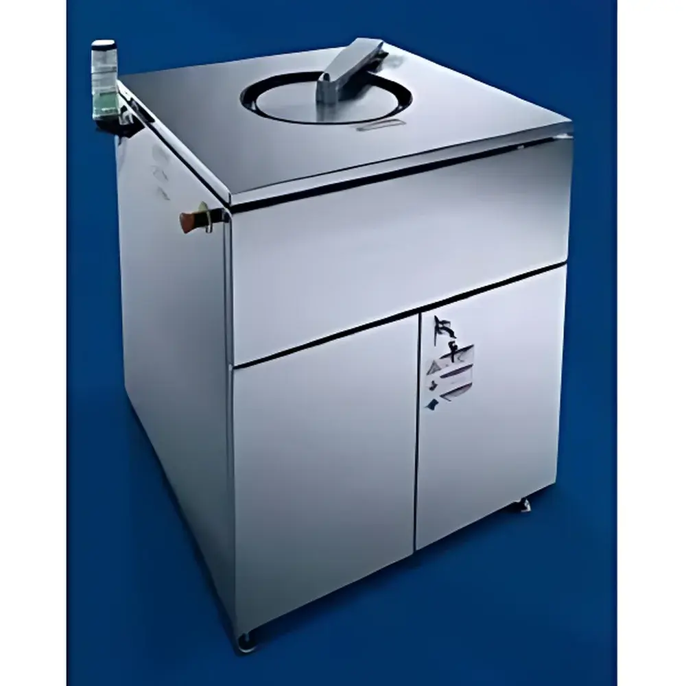
| Dimensions (W × H × D) | 70 × 105 × 92.5 cm |
| Uniformity | < ±1% across 200 mm wafers (typical, SiO₂ on Si) |
Overview
The PICOSUN® R-Series Atomic Layer Deposition (ALD) system is a benchtop-to-production scalable platform engineered for precision thin-film synthesis in semiconductor R&D, MEMS fabrication, and advanced materials development. Based on the foundational principles of self-limiting surface reactions—first demonstrated by Dr. Tuomo Suntola in 1974—the R-Series implements true thermal ALD with sub-angstrom thickness control, atomic-scale conformality, and exceptional run-to-run reproducibility. Its modular reactor architecture supports both batch and single-wafer processing configurations, enabling seamless transition from process development to pilot-line integration. Designed and manufactured in Espoo, Finland, the system adheres to ISO 9001-certified production protocols and incorporates fail-safe gas delivery, real-time pressure monitoring, and Class 100 cleanroom-compatible construction.
Key Features
- Modular reactor chamber options: Small-, medium-, and large-volume configurations fabricated from electropolished 316 stainless steel, titanium, nickel, aluminum, or fused quartz—selected per precursor compatibility and thermal stability requirements.
- Thermal ALD operation up to 500 °C, with rapid thermal ramping (≤10 °C/s) and isothermal stability of ±0.5 °C over extended cycles.
- 2–6 independent precursor delivery lines supporting gaseous, bubbled liquid, and solid-source (e.g., powder or pellet) chemistries—including metal halides, alkylamides, and oxygen/nitrogen plasma co-reactants (with optional RF module).
- Picoloader™ manual load-lock system featuring integrated pre-vacuum chamber (base pressure <1×10⁻⁶ mbar), gate valve isolation, and wafer alignment stage—enabling atmospheric break-free sample exchange and minimizing chamber contamination.
- Integrated vacuum infrastructure: Dry scroll pump (30–80 m³/h pumping speed), N₂/Ar carrier gas supply (≥2 slm, 99.999% purity), compressed air interface (4–5.5 bar), and dedicated exhaust routing for both pump and precursor cabinets.
- Robust electrical design: Universal 100–240 V, 50/60 Hz, 1- or 3-phase input; total power draw ≤3.7 kW; no external cooling water required.
Sample Compatibility & Compliance
The R-Series accommodates substrates from 50 mm (2″) to 200 mm (8″) diameter, including silicon, III–V compounds (GaAs, InP), sapphire, glass, flexible polymers (e.g., PI, PET), and high-aspect-ratio nanostructures (e.g., nanowires, porous anodic alumina). Film uniformity is validated per SEMI F20 and ASTM F39–22 standards, with typical thickness variation <±1% across full 200 mm wafers for Al₂O₃, TiO₂, and SiO₂ layers. The system meets CE marking requirements and complies with IEC 61000-6-2 (EMC immunity) and IEC 61000-6-4 (EMC emission) directives. Optional audit-ready software packages support 21 CFR Part 11 compliance for GMP/GLP environments, including electronic signatures, change control logs, and full data traceability.
Software & Data Management
PICOSUN’s proprietary PicoSoft™ control suite provides deterministic recipe execution, real-time process visualization (pressure, temperature, valve status), and automated parameter logging at 100 ms resolution. All process data—including layer counts, pulse durations, purge times, and chamber diagnostics—are stored in encrypted SQLite databases with configurable export (CSV, XML, HDF5). Remote monitoring via secure HTTPS API enables integration into factory MES systems. Audit trail functionality records user actions, parameter modifications, and system events with timestamped, non-erasable entries—fully aligned with FDA 21 CFR Part 11 and EU Annex 11 expectations.
Applications
- Semiconductor gate dielectrics (HfO₂, Al₂O₃, La₂O₃) and high-k/metal gate stacks.
- MEMS passivation layers (AlN, SiNₓ) with pinhole-free coverage on complex topographies.
- Perovskite solar cell electron/hole transport layers and interfacial stabilization films.
- Biomedical coatings (TiO₂, ZnO) on implantable devices requiring nanoscale thickness fidelity and cytocompatibility.
- Atomic-scale encapsulation of quantum dots, 2D materials (MoS₂, h-BN), and catalytic nanoparticles.
FAQ
What substrate sizes does the R-Series support?
Standard configurations handle 50–150 mm wafers; 200 mm (8″) processing is available upon request with Picoloader™ load-lock upgrade.
Is plasma-enhanced ALD supported?
Yes—optional RF-powered remote plasma source (13.56 MHz) can be integrated for low-temperature PE-ALD of nitrides, oxides, and fluorides.
How is precursor consumption monitored?
Mass flow controllers (MFCs) with NIST-traceable calibration provide real-time precursor usage tracking; optional residual gas analysis (RGA) module enables in-situ byproduct detection.
Can the system be upgraded post-purchase?
All R-Series platforms are designed for field-upgradability—including additional precursor lines, larger reactors, plasma modules, and software license tiers.
What service and support is included?
Standard warranty covers 12 months parts and labor; extended service contracts include preventive maintenance, remote diagnostics, and on-site engineer response within 72 business hours (EMEA/APAC regions).


