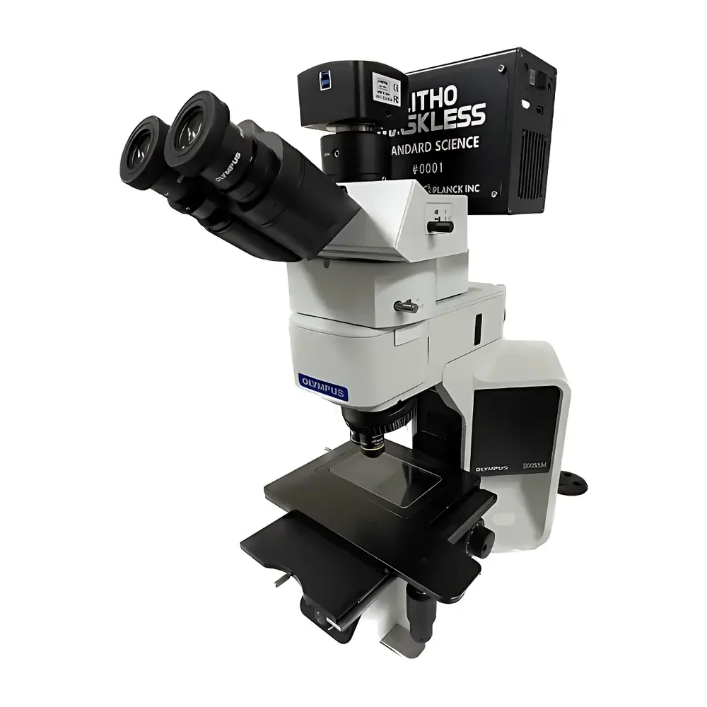
Planck LithoMaskless Direct Write Lithography System
| Brand | AYAO Instruments |
|---|---|
| Origin | South Korea |
| Manufacturer Type | Authorized Distributor |
| Product Origin | Imported |
| Model | LithoMaskless |
| Exposure Mode | Projection-Based |
| Resolution | 0.5 µm |
| Light Source | UV LED |
| Wavelength Options | 365 nm / 385 nm / 405 nm |
| Maximum Exposure Area | 100 mm × 100 mm |
| DMD Chip Size | 0.65-inch |
| Compatibility | Broad photoresist & substrate support (Si, SiO₂, glass, quartz, flexible polymers) |
| Alignment Method | Integrated high-magnification optical alignment with real-time feedback |
Overview
The Planck LithoMaskless Direct Write Lithography System is a precision projection-based photolithography platform engineered for maskless, digital patterning of microstructures on planar substrates. Unlike conventional contact or proximity lithography tools, it eliminates the need for physical photomasks by leveraging a 0.65-inch Digital Micromirror Device (DMD) as a dynamic, programmable spatial light modulator. The system operates on the principle of digital light projection: UV photons from wavelength-tunable LEDs (365 nm, 385 nm, or 405 nm) are reflected off individually addressable micro-mirrors—each corresponding to a pixel in the pattern—and focused through a high-NA vertical microscope objective onto the photoresist-coated substrate. This enables true sub-micron resolution (≤0.5 µm half-pitch) with high positional fidelity and excellent dose uniformity across the full 100 mm × 100 mm exposure field. Designed for research-grade flexibility and process repeatability, the LithoMaskless system bridges the gap between academic prototyping and low-volume fabrication in cleanroom-adjacent environments.
Key Features
- Projection-based maskless architecture using a high-speed, industrial-grade 0.65-inch DMD for real-time pattern modulation
- Triple-wavelength UV LED illumination (365/385/405 nm) optimized for broad photoresist compatibility—including SU-8, AZ series, PMMA, and novel 2D-material-compatible resists
- Sub-500 nm resolution capability verified under standard lithographic conditions (e.g., 1.5 µm thick AZ 5214E, post-bake development)
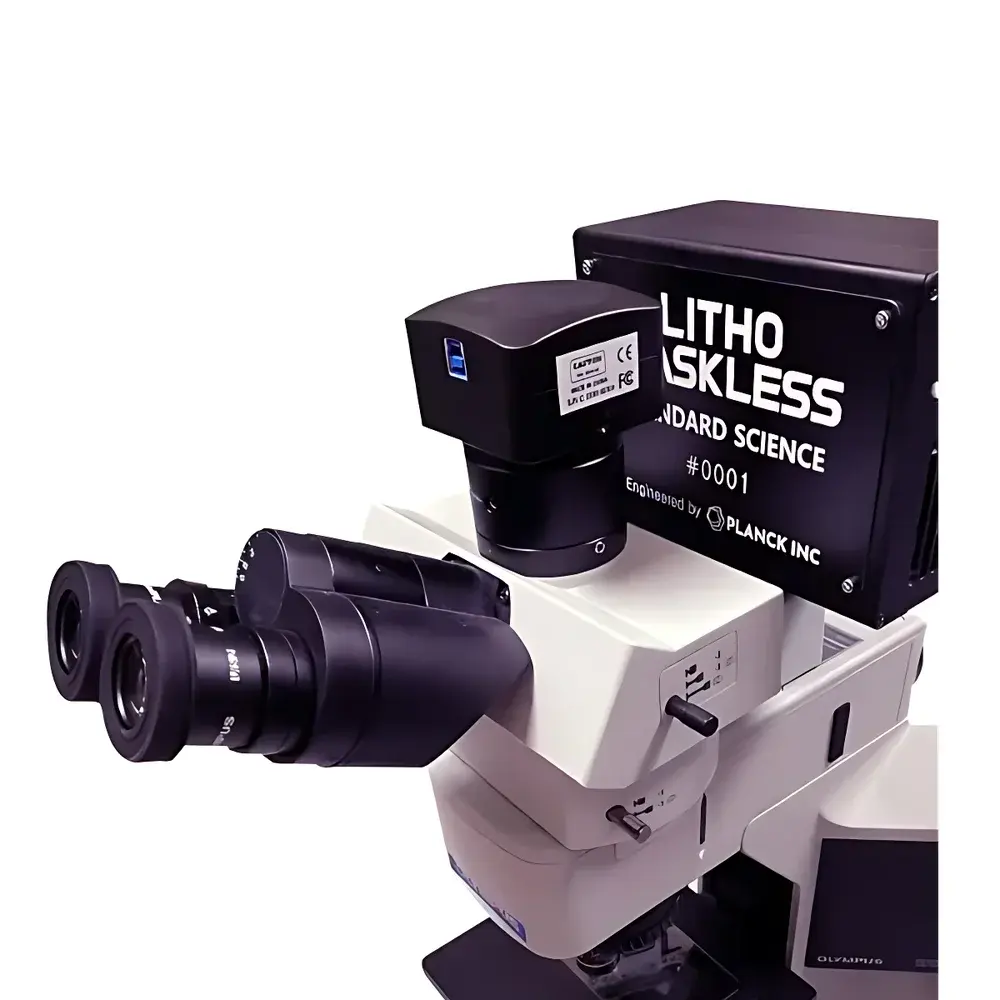
- Integrated upright microscope alignment subsystem with motorized Z-focus, live CCD imaging, and sub-pixel crosshair overlay for precise layer-to-layer registration
- AI-driven intensity compensation algorithm that dynamically adjusts mirror dwell time per pixel to correct for optical vignetting and DMD non-uniformity—ensuring ±3% dose variation across the full exposure area
- Modular mechanical design supporting vacuum chucking, thermal stage options (±5 °C stability), and optional environmental enclosure for humidity-sensitive processes
Sample Compatibility & Compliance
The LithoMaskless system accommodates rigid and semi-flexible substrates up to 150 mm in diameter and 10 mm in thickness—including silicon wafers (100–300 mm), fused silica, borosilicate glass, sapphire, ITO-coated PET, and oxidized metal foils. It supports both positive and negative tone resists, including those formulated for low-dose EUV alternatives and emerging 2D material transfer protocols. All optical and motion components comply with IEC 61000-6-2 (EMC immunity) and IEC 60825-1 (laser product safety classification, applicable to UV LED sources). While not certified for full GMP manufacturing, its software architecture supports audit-ready operation: all exposure parameters (wavelength, dose, focus offset, alignment coordinates) are timestamped and logged in binary + CSV format, enabling traceability per ISO 9001 and GLP documentation requirements.
Software & Data Management
Control is executed via PlanckLitho™ v4.x, a Windows-based application built on Qt and Python (PyQt5, NumPy, OpenCV). The GUI provides intuitive vector-based pattern import (DXF, GDSII, SVG), rasterization engine with anti-aliasing and proximity effect correction (PEB-aware dose modulation), and real-time exposure monitoring with histogram-based dose feedback. Pattern files are compiled into optimized bitmaps stored in non-volatile memory onboard the DMD controller, ensuring deterministic timing independent of host PC latency. All session logs, alignment records, and calibration profiles are saved in a structured SQLite database with configurable auto-backup to network shares. For regulated environments, optional FDA 21 CFR Part 11-compliant modules are available—including electronic signatures, role-based access control, and immutable audit trails.
Applications
- Two-dimensional materials device fabrication: patterning of MoS₂/WSe₂ heterojunctions, graphene electrodes, h-BN encapsulation windows, and van der Waals heterostructure alignment markers
- MEMS and microfluidics: rapid prototyping of piezoresistive pressure sensors, electrokinetic micropumps, droplet-based lab-on-chip channels, and integrated electrode arrays
- Academic and industrial R&D: iterative design validation for photonics (gratings, metasurfaces), plasmonics, and quantum dot arrays—without mask fabrication lead time or cost
- Hybrid integration workflows: direct-write patterning aligned to pre-fabricated CMOS or GaN test structures for heterogeneous packaging and interconnect definition
FAQ
What photoresists are validated for use with the LithoMaskless system?
Standard g-line and i-line resists (e.g., AZ 1518, SU-8 2005/2010, ma-N 2401) have been experimentally characterized at 365 nm and 405 nm. High-resolution performance with CALIX and ZEP-520A has also been demonstrated under optimized dose and PEB conditions.
Can the system perform multi-layer alignment?
Yes—the integrated optical alignment module supports manual and semi-automated layer-to-layer registration with ≤±0.3 µm overlay accuracy (3σ) using fiducial-based image correlation and sub-pixel interpolation.
Is vacuum or nitrogen purge supported?
The base configuration includes a sealed optical path; optional vacuum chucking (10⁻² mbar) and N₂ purge ports are available for oxygen-sensitive resists or high-aspect-ratio development.
How is resolution verified and maintained?
Resolution is confirmed using NIST-traceable linewidth standards (e.g., SEMATECH LER test patterns) and calibrated via periodic MTF measurements using knife-edge scans. DMD mirror calibration is performed automatically during system startup.
Does the system support grayscale or variable-dose lithography?
Yes—dwell-time modulation per pixel enables continuous-tone exposure, facilitating fabrication of diffractive optical elements, micro-lens arrays, and topography-defined relief structures.


