point electronic 3D Calibration Kit for Electron Microscopy and Scanning Probe Microscopy
| Brand | point electronic |
|---|---|
| Origin | Germany |
| Model | 3D Calibration Kit |
| Compliance | VDI/VDE 2656 |
| Software | microCal Calibration Suite |
| Compatibility | SEM, AFM, CLSM, 3D-SEM |
| Calibration Type | Geometric Metrology (X/Y/Z Scale, Shear, Coupling) |
| Traceability | NIST-traceable reference data provided |
Overview
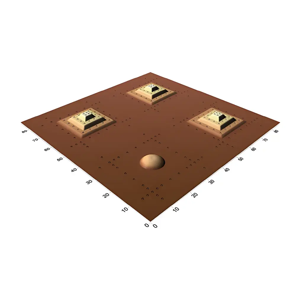
The point electronic 3D Calibration Kit is a metrologically traceable hardware–software system engineered for geometric calibration of scanning electron microscopes (SEM), atomic force microscopes (AFM), confocal laser scanning microscopes (CLSM), and 3D-SEM platforms. It implements a reference-based, image-processing-driven methodology compliant with VDI/VDE 2656 Part 1 (“Calibration of Scanning Probe Microscopes for Geometrical Quantities”), enabling quantitative assessment and correction of spatial distortions across all three orthogonal axes (X, Y, Z). Unlike conventional 2D grating standards, this kit addresses coupled geometric errors—including lateral scale anisotropy, axial magnification drift, and inter-axis shear—by leveraging a physically characterized 3D reference standard with certified topographic features. The system operates on the principle of comparative metrology: acquired micrographs of the calibration standard are algorithmically registered against its NIST-traceable reference dataset, permitting statistical derivation of pixel-to-real-world scaling factors, rotation matrices, and affine transformation parameters.
Key Features
- Simultaneous determination of lateral (X/Y) and vertical (Z) scale factors with quantified uncertainty budgets
- Comprehensive characterization of cross-axis coupling effects—including XY–Z shear, orthogonality deviation, and non-linear warping
- Automated parameter extraction via microCal software using robust sub-pixel feature detection and least-squares registration
- Hardware–software co-validation architecture: each calibration standard ships with digitally signed, version-controlled reference data aligned to ISO/IEC 17025 traceability requirements
- Modular design supporting optional spherical segment inserts for BSE detector alignment optimization in segmented backscattered electron imaging
- Platform-agnostic software interface compatible with TIFF, BMP, and vendor-specific raw formats (e.g., Zeiss .tif, Thermo Fisher .ser, Bruker .bmf)
Sample Compatibility & Compliance
The included 3D calibration standard consists of a silicon-based substrate fabricated via deep reactive ion etching (DRIE), featuring precisely defined step heights (nominal 100 nm–5 µm), periodic line gratings (pitch: 1–10 µm), and fiducial markers with sub-10 nm edge roughness. All physical dimensions are certified per DIN EN ISO 17025 by an accredited metrology laboratory in Germany. The kit satisfies regulatory expectations for instrument qualification under GLP and GMP environments, particularly where dimensional stability and measurement traceability are mandated—for example, in semiconductor process control, medical device surface characterization (ISO 10993-22), or ASTM E2981-20-compliant nanoscale roughness verification. VDI/VDE 2656 compliance ensures documented procedures for uncertainty estimation, environmental influence evaluation (temperature, vibration), and re-calibration intervals.
Software & Data Management
microCal is a standalone Windows application built on Qt and OpenCV, designed for audit-ready calibration workflows. It performs batch processing of multi-frame acquisitions, applies statistical outlier rejection (Grubbs’ test), and computes full 3×3 affine transformation matrices. Each calibration session generates a machine-readable JSON report containing all derived parameters, confidence intervals, residual error maps, and metadata (operator ID, timestamp, microscope model, detector settings). The software supports FDA 21 CFR Part 11-compliant user authentication, electronic signatures, and immutable audit trails when deployed with enterprise license management. Exported correction parameters integrate directly into common microscopy acquisition suites (e.g., SmartSEM, Gwyddion, MountainsMap) or can be applied post-acquisition via Python API bindings.
Applications
- Quantitative height metrology in failure analysis labs performing cross-sectional SEM or FIB-SEM tomography
- Validation of Z-resolution claims for high-resolution SEMs operating below 1 kV acceleration voltage
- Traceable roughness (Sa, Sq) and waviness (Wa, Wq) measurements per ISO 25178-2 in R&D and quality assurance
- Inter-laboratory comparison studies requiring SI-traceable length standards at sub-micron scales
- Verification of automated stage positioning accuracy in correlative light–electron microscopy (CLEM) workflows
- Preventive maintenance documentation for ISO 9001-certified manufacturing facilities
FAQ
Is the calibration standard reusable across multiple instruments and laboratories?
Yes—the silicon reference standard is chemically inert, vacuum-compatible, and mechanically stable under routine handling. Its reference dataset remains valid for the lifetime of the artifact unless physically damaged.
Does microCal support real-time correction during image acquisition?
No—microCal operates offline on saved images. Real-time correction requires integration with vendor SDKs, which is available under extended support contracts.
Can the kit calibrate beam-induced drift or thermal expansion artifacts?
It does not compensate for dynamic artifacts. However, it quantifies static geometric distortions that dominate measurement uncertainty budgets in most high-precision applications.
What documentation accompanies delivery?
Each kit includes a Certificate of Calibration (with uncertainty statement), VDI/VDE 2656 conformance declaration, microCal installation media, and a secure digital repository link for reference data updates.


