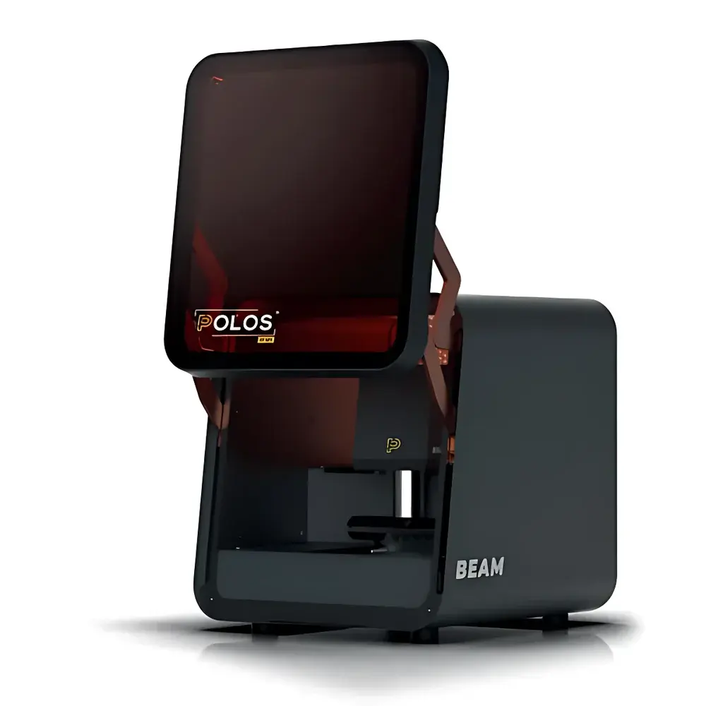
POLOS® BEAM Desktop Maskless Lithography System
| Brand | SPS-POLOS |
|---|---|
| Origin | Germany |
| Manufacturer Type | Authorized Distributor |
| Category | Imported Instrument |
| Model | BEAM |
| Resolution | 0.8 µm (CD) |
| Light Source | Laser Galvanometer + 405 nm Laser Diode |
| Exposure Field | 150 mm × 150 mm |
| Substrate Compatibility | 4″–6″ wafers |
| Focus Actuation | Piezoelectric auto-focus with closed-loop optics (<1 s settling time) |
| Alignment | Semi-automatic multi-layer collimation (completed in minutes) |
| Compatible Resist | AZ5214E |
| Software Interface | GDSII-native GUI with wafer-level navigation, layer overlay, and CNC-style motion control |
Overview
The POLOS® BEAM Desktop Maskless Lithography System is a compact, high-precision direct-write lithography platform engineered for rapid prototyping and low-volume microfabrication in academic, R&D, and pilot-line environments. Unlike conventional mask-based photolithography, the BEAM system eliminates the need for physical photomasks by employing a focused 405 nm ultraviolet laser beam—scanned via high-speed galvanometric mirrors—to expose photoresist directly with sub-micron spatial fidelity. The optical engine achieves diffraction-limited spot size, enabling critical dimension (CD) control down to 0.8 µm on silicon wafers up to 6 inches in diameter. Its integrated piezoelectric autofocus mechanism, coupled with closed-loop focusing optics, ensures consistent resist exposure across non-planar or warped substrates, delivering high reproducibility without manual intervention. Designed as a turnkey desktop instrument—smaller than a standard PC tower—the BEAM bridges the gap between research-grade flexibility and production-relevant resolution, supporting iterative device development without mask fabrication lead times or associated costs.
Key Features
- Sub-micron resolution: Achieves <0.8 µm CD on 4″–6″ wafers using AZ5214E positive tone resist under optimized process conditions.
- Full-field exposure capability: 150 mm × 150 mm maximum writing area, scalable via precision motorized stage stitching for seamless large-area patterning.
- Real-time autofocus: Closed-loop piezoelectric actuator delivers focus stabilization in under 1 second, compensating for substrate topography variations up to ±15 µm.
- Rapid pattern throughput: Full-field exposure completed in <2 seconds per field (100 µm × 100 µm), enabling efficient iteration during design validation.
- Multi-layer alignment: Semi-automated collimation routine supports accurate registration across ≥3 layers within minutes, with visual overlay of GDSII layers in real time.
- Compact industrial design: All-in-one benchtop footprint (W×D×H: 420 × 480 × 360 mm), CE-compliant, air-cooled, and compatible with standard cleanroom Class 1000 environments.
Sample Compatibility & Compliance
The BEAM system accommodates standard semiconductor substrates including silicon, fused silica, SOI, and glass wafers from 100 mm (4″) to 150 mm (6″) diameter. It supports both spin-coated and spray-applied photoresists; validated processes include AZ5214E, SU-8, and PMMA. Chuck vacuum hold-down ensures minimal thermal drift during exposure. The system complies with IEC 61000-6-3 (EMC emission) and IEC 61000-6-2 (immunity), and meets laser safety Class 1 requirements per IEC 60825-1 when interlocked. While not certified for full GMP manufacturing, its software architecture supports audit trails and user-access controls aligned with GLP documentation practices—enabling traceability for qualification studies per ISO/IEC 17025 and ASTM F2659.
Software & Data Management
The BEAM Control Suite is a native GDSII-compatible platform built on a deterministic real-time kernel. It provides hierarchical pattern import, layer-by-layer alignment preview, and wafer-level navigation via interactive mini-map interface—functionally analogous to CNC coordinate programming. All exposure parameters (dose, scan velocity, focus offset, layer stack order) are stored in XML-based project files with SHA-256 checksums for version integrity. Export options include OASIS, CIF, and SVG for cross-platform verification. The software logs timestamped operation records—including stage position, laser power feedback, and autofocus status—for post-process correlation. Optional integration with LabVIEW or Python APIs enables automated batch processing and metrology loop closure with external CD-SEM or AFM tools.
Applications
- MEMS and NEMS device prototyping: Fabrication of cantilevers, resonators, and microfluidic channels with submicron feature definition.
- Photonic integrated circuit (PIC) test structures: Rapid iteration of grating couplers, waveguide bends, and ring resonators on silicon photonics platforms.
- Quantum device research: Patterning of superconducting qubit architectures, Josephson junction arrays, and gate-defined quantum dots.
- Micro-opto-electro-mechanical systems (MOEMS): Direct-write of diffractive optical elements (DOEs), microlens arrays, and tunable mirror actuators.
- Academic microfabrication labs: Teaching tool for lithography fundamentals, resist characterization, and process window analysis without mask inventory overhead.
FAQ
What substrates and resists are officially supported?
Silicon, SiO₂, quartz, and glass wafers (4″–6″) are fully supported. AZ5214E is the reference resist; process recipes for SU-8 2000 series and PMMA 950K are available upon request.
Is the system compatible with existing cleanroom infrastructure?
Yes—it operates at ambient temperature and pressure, requires only 110–240 VAC input, and generates no hazardous exhaust. Vibration isolation feet are included for standard optical tables.
Can the BEAM perform grayscale or variable-dose lithography?
No—this is a binary exposure system optimized for high-fidelity vector scanning. Grayscale functionality is not implemented in current firmware.
How is stage calibration maintained over time?
A built-in interferometric encoder verifies positional accuracy before each job. A quarterly recalibration kit (traceable to NIST standards) is available through SPS-POLOS service contracts.
Does the software support remote operation or network deployment?
Yes—via secure SSH tunneling or VLAN-isolated Ethernet connection. Multi-user license tiers allow concurrent access with role-based permissions (Operator, Engineer, Admin).


