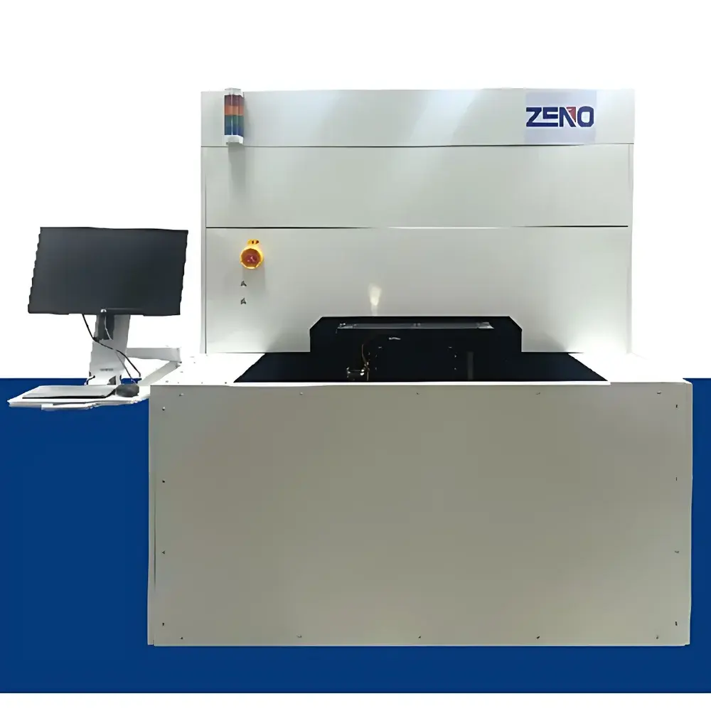
PULSAR Series Wafer Defect Inspection System
| Brand | ZENO |
|---|---|
| Origin | Shanghai, China |
| Model | PULSAR L-Series & PULSAR H-Series |
| Category | Semiconductor Wafer Defect Detection Instrument |
| Manufacturer Type | Authorized Distributor |
| Regional Classification | Domestic (China) |
| Pricing | Upon Request |
Overview
The PULSAR Series Wafer Defect Inspection System is a purpose-built optical inspection platform engineered for front-end semiconductor manufacturing environments. It employs high-contrast brightfield and darkfield imaging combined with advanced pixel-level signal processing to detect, classify, and spatially localize physical defects on bare and patterned silicon wafers. Designed specifically for applications in wafer-level packaging (WLP), panel-level packaging (PLP), and advanced node front-end-of-line (FEOL) process monitoring, the system operates on the principle of scattering-based defect contrast enhancement—leveraging optimized illumination geometry, high-numerical-aperture optics, and calibrated photometric response to resolve sub-micron anomalies including particles, scratches, pits, bridging, and missing patterns. Its architecture supports both inline process control and offline failure analysis workflows, delivering repeatable detection sensitivity across 200 mm, 300 mm, and emerging 450 mm wafer formats.
Key Features
- Multi-resolution imaging capability: Configurable optical paths enabling scalable resolution from 1.0 µm (L-Series) to ≤0.35 µm (H-Series) at full-wafer throughput
- Real-time parallel image processing engine: FPGA-accelerated pipeline supporting >120 fps frame rate at 4K × 4K sensor resolution
- Autonomous defect classification: Rule-based and supervised machine learning algorithms trained on industry-standard defect libraries (e.g., SEMI E142, ITRS defect taxonomy)
- Sub-pixel centroid localization: Achieves ≤±0.15 µm positional accuracy via centroid interpolation and stage encoder synchronization
- Modular hardware design: Interchangeable objective turrets, multi-spectral LED illumination modules (365 nm–940 nm), and vacuum-compatible chuck options
- Integrated metrology correlation: Direct coordinate mapping to CD-SEM, AFM, or FIB-SEM tools via standardized SEMI E39 (SECS/GEM) and E148 (Equipment Data Acquisition) interfaces
Sample Compatibility & Compliance
The PULSAR Series accommodates standard silicon wafers (200 mm, 300 mm), compound semiconductor substrates (SiC, GaN, InP), and advanced packaging panels up to 600 × 600 mm (PLP mode). Chuck thermal stability is maintained within ±0.3 °C over 8-hour operation to minimize thermal drift-induced false positives. The system complies with SEMI S2/S8 safety standards and meets electromagnetic compatibility requirements per CISPR 11 Class A. All software modules adhere to data integrity principles aligned with FDA 21 CFR Part 11 for electronic records and signatures—supporting audit trails, user role-based access control (RBAC), and secure data export in ASTM E2797-compliant XML/CSV formats. It is validated for use in ISO 9001-certified fabs and supports GLP/GMP-aligned qualification protocols including IQ/OQ/PQ documentation templates.
Software & Data Management
ZENO VisionSuite™ is the proprietary inspection software platform, built on a deterministic real-time OS kernel and featuring a modular architecture compliant with SEMI EDA/Interface A standards. It provides unified control of imaging, motion, lighting, and analysis subsystems through a centralized GUI with customizable workflow scripting (Python 3.9 API). Defect data—including XY coordinates, size, shape descriptors, intensity histograms, and classified type—is stored in an embedded SQLite database with optional integration into factory MES via OPC UA or RESTful webhooks. Raw image archives are retained with lossless compression (PNG-24 + metadata embedding) and support automated backup to NAS or cloud object storage (AWS S3, Azure Blob) with AES-256 encryption. Version-controlled software updates follow IEEE 1012-compliant verification procedures, and all analysis algorithms undergo periodic revalidation per internal SOP-INS-007.
Applications
- Pre- and post-lithography defect screening for 28 nm to 3 nm node processes
- Particle monitoring during chemical mechanical polishing (CMP) and etch process qualification
- Defect root-cause analysis in WLP redistribution layer (RDL) and bump formation
- Panel-level defect mapping for fan-out wafer-level packaging (FOWLP) and chiplet assembly
- Qualification of EUV mask blanks and pellicle integrity verification
- Failure analysis support for electrical test yield loss correlation (e.g., linking killer defects to parametric test outliers)
FAQ
Does the PULSAR Series support automated defect review with integrated SEM correlation?
Yes—via SEMI E148-compliant equipment data acquisition and coordinate transformation matrix calibration, enabling direct navigation to defect sites on compatible CD-SEM platforms.
What wafer handling options are available for high-throughput production environments?
Standard configurations include robotic arm integration (SEMI E47.1 compliant), FOUP/FOSB load ports, and dual-cassette autoloaders with SMIF interface support.
Is the system qualified for use in Class 1 cleanroom environments?
The PULSAR H-Series is rated ISO Class 1 (per ISO 14644-1) when operated with HEPA-filtered laminar airflow enclosures and static-dissipative material handling components.
Can inspection recipes be transferred between L-Series and H-Series platforms?
Yes—recipe portability is ensured through ZENO’s unified VisionSuite™ framework; however, resolution-dependent parameters require validation per SEMI E139 guidelines.
How is measurement traceability maintained for defect size reporting?
All optical magnifications are calibrated using NIST-traceable Ronchi rulings and verified per ISO/IEC 17025-accredited procedures; pixel-to-µm conversion factors are logged with timestamped calibration certificates.


