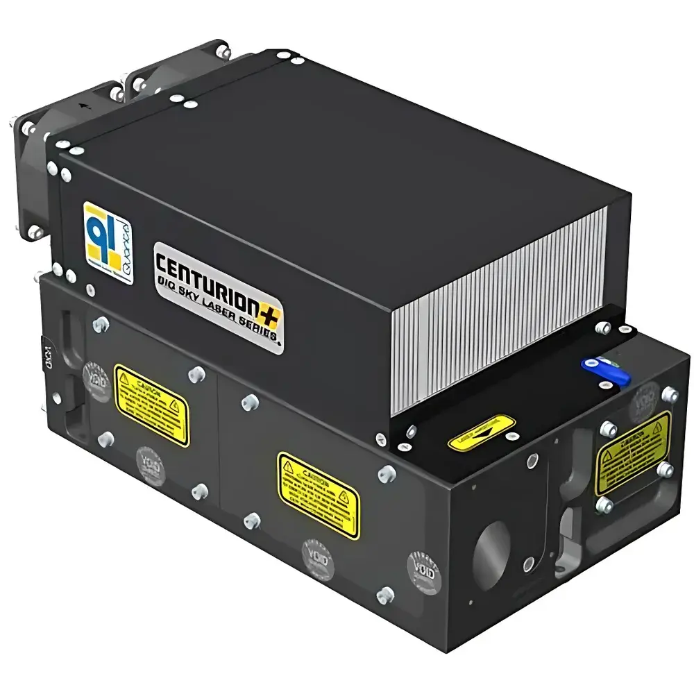
Quantel 532 nm DPSS Laser Repair Module for LCD/OLED Display Panel Rework
| Brand | Quantel |
|---|---|
| Origin | France |
| Model | 532 |
| Laser Type | Diode-Pumped Solid-State (DPSS) |
| Wavelengths | 1064 nm / 532 nm / 355 nm / 266 nm |
| Pulse Repetition Rate | 1–100 Hz |
| Pulse Width | 12 ± 2 ns |
| Power Supply | 48 V DC |
| Construction | Monolithic aerospace-grade aluminum housing, N₂-purged and fully rigidized optical cavity |
| Key Innovations | Suppressed first-pulse overshoot, square-top uniform beam profile |
| Application Scope | Array, Color Filter (COA), Cell, and Module-level repair in TFT-LCD and AMOLED manufacturing |
Overview
The Quantel 532 nm DPSS Laser Repair Module is an industrial-grade optical subsystem engineered specifically for precision defect mitigation in flat-panel display (FPD) manufacturing. It operates on the principle of localized photothermal ablation and micro-welding, leveraging nanosecond-pulsed solid-state laser radiation to selectively modify conductive traces (e.g., ITO lines), isolate defective pixels, or sever shorted electrodes without inducing thermal damage to underlying layers. Designed for integration into automated AOI-coupled repair stations, this module delivers deterministic energy deposition at sub-10 µm spatial resolution—enabling reliable correction of bright spots, dark spots, flicker defects, and fragmented pixel anomalies in both LCD and OLED backplane architectures. Its compact monolithic design, sealed nitrogen environment, and DC-powered architecture ensure long-term operational stability in cleanroom environments compliant with ISO Class 5 (Class 100) standards.
Key Features
- Four-wavelength DPSS laser platform (1064/532/355/266 nm) with synchronized harmonic generation for process flexibility across different layer materials (e.g., Mo, Al, ITO, organic emissive layers)
- Stable pulse-to-pulse energy output (< ±1.5% RMS over 8 hours), achieved via rigidized cavity design and active thermal management
- Square-top beam profile with <5% intensity variation across 90% of the defined aperture—eliminating Gaussian edge effects that cause under-/over-processing
- No-first-pulse anomaly suppression technology, ensuring consistent ablation threshold behavior from the initial shot
- Integrated optical head featuring motorized wavelength selection, precision variable attenuator (0.1–100% transmission), programmable slit-based beam shaping, and co-aligned white-light illumination for real-time process monitoring
- High-speed autofocus subsystem with closed-loop piezoelectric Z-stage (±50 µm range, 50 nm repeatability) enabling dynamic focus compensation during high-throughput repair sequences
Sample Compatibility & Compliance
The module supports direct integration with standard FPD handling platforms for glass substrates up to Gen 8.5 (2200 × 2500 mm). It is compatible with common display stack architectures including a-Si, LTPS, and IGZO TFT backplanes; RGBW and WRGB OLED emitter stacks; and color filter arrays fabricated via photolithography or inkjet printing. All optical components meet RoHS Directive 2011/65/EU and REACH Annex XVII requirements. System-level validation data are traceable to NIST-traceable radiometric calibration standards. The laser safety architecture conforms to IEC 60825-1:2014 Class 4 specifications, with interlocked enclosure interfaces supporting EN 61496-1 machine guarding compliance.
Software & Data Management
Control firmware supports SECS/GEM protocol for factory automation integration and provides API-level access via TCP/IP for custom MES/SCADA linkage. Repair log files include timestamped metadata (pulse count, energy per shot, focal position, wavelength selected, substrate ID), stored in CSV and SQLite formats. Audit trails comply with FDA 21 CFR Part 11 requirements when deployed in regulated GMP environments, including electronic signature support, user role-based permissions, and immutable event logging. Optional software modules enable statistical process control (SPC) charting of repair yield metrics and correlation with inline AOI defect maps.
Applications
- Array-level repair: Short-circuit isolation in gate/source/drain lines; redundant line cutting in LTPS driver circuits
- Color filter (COA) repair: Selective removal of metal light-shielding layers without damaging underlying photoresist or black matrix
- Cell-level rework: Pixel electrode trimming in AMOLED panels to suppress leakage current and improve contrast ratio
- Module-level bonding: Micro-welding of flexible printed circuit (FPC) connectors to panel edge terminals with minimal heat-affected zone
- Defect grading mitigation: Conversion of Grade A2/B panels to Grade A1 through systematic bright-spot neutralization and dark-spot activation
FAQ
What substrates and layer thicknesses can this module process?
It supports glass substrates (0.4–1.1 mm thickness) and polyimide-based flexible OLED carriers. Typical target layers include ITO (30–150 nm), Mo (50–200 nm), Al (100–300 nm), and organic emissive layers (80–200 nm), with ablation thresholds validated per material stack configuration.
Is the system compatible with existing AOI inspection platforms?
Yes—standard Ethernet and RS-232 interfaces allow bidirectional communication with major AOI vendors (e.g., Orbotech, Applied Materials, SCREEN). Coordinate mapping between defect coordinates and laser positioning is handled via configurable transformation matrices.
Does the module require water cooling or external chillers?
No—thermal management is passive and conduction-based, enabled by the high-conductivity aluminum monoblock housing. Ambient operating temperature range is 20–25 °C with ≤60% RH non-condensing.
Can the system be validated for ISO 13485 or IATF 16949 production lines?
Yes—full IQ/OQ documentation packages are available upon request, including installation qualification checklists, operational boundary testing reports, and metrological traceability statements aligned with ISO/IEC 17025-accredited calibration labs.


