Quantum Design FusionScope Hybrid SEM-AFM Microscope
| Brand | Quantum Design |
|---|---|
| Origin | USA |
| Manufacturer Type | Manufacturer |
| Origin Category | Imported |
| Model | FusionScope |
| Instrument Type | Floor-standing / Conventional Large-scale |
| Electron Gun Type | Thermal Field Emission |
| Magnification Range | 25× – 200,000× |
| Acceleration Voltage | 3.5 kV – 15 kV |
| Maximum Sample Diameter | 20 mm |
| Standard Detector System | In-chamber Secondary Electron (SE) Detector |
| AFM Scan Range (XY) | 22 × 22 µm (closed-loop) |
| AFM Z-Range | 15 µm |
| AFM Imaging Noise | <50 pm @ 1 kHz |
| AFM Probe Type | Self-sensing piezoresistive cantilever |
| AFM Modes | Contact, Dynamic (Tapping), FIRE, MFM, C-AFM, EFM |
| SEM Beam Current | 5 pA – 2.5 nA (typ. 300 pA) |
| Chamber Vacuum | 1–10 µTorr |
| Pump-down Time | <5 min |
| Sample Stage Tilt | −10° to +80° |
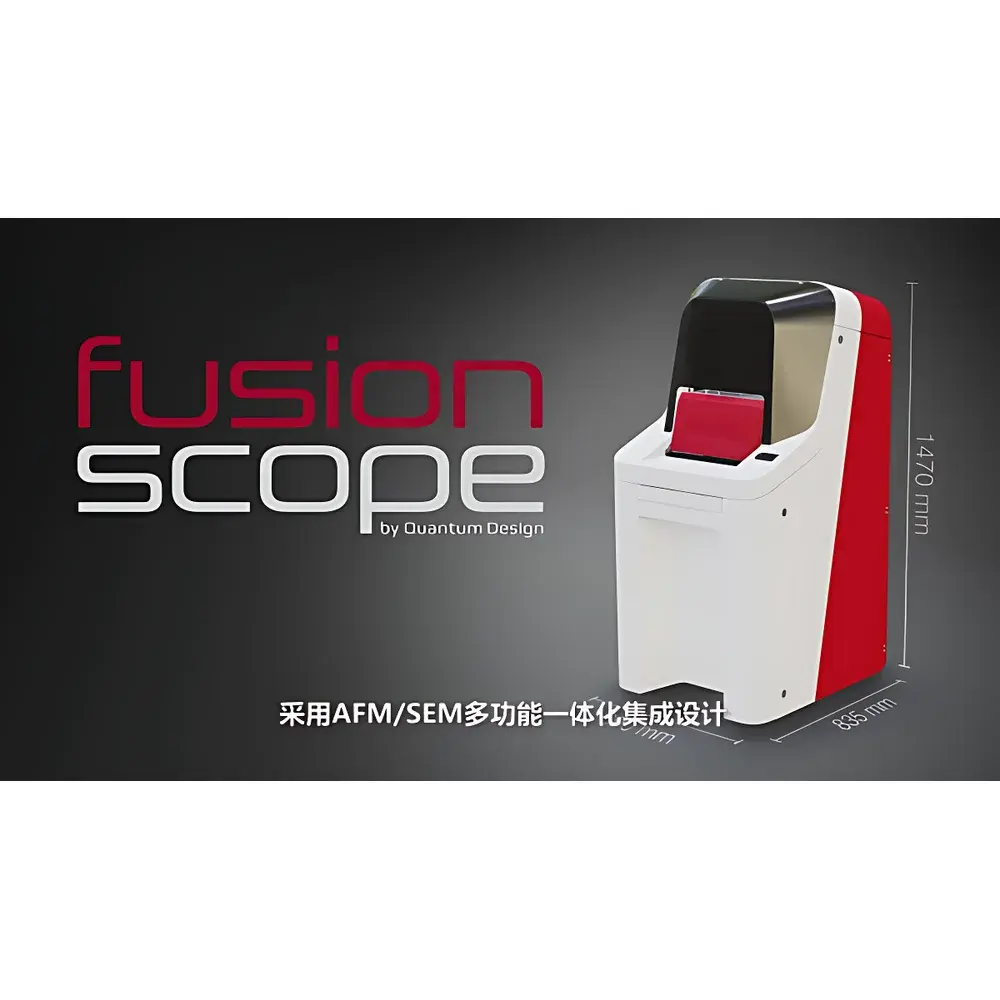
| Dimensions (W×D×H) | 690 × 835 × 1470 mm |
| Weight | 330 kg |
Overview
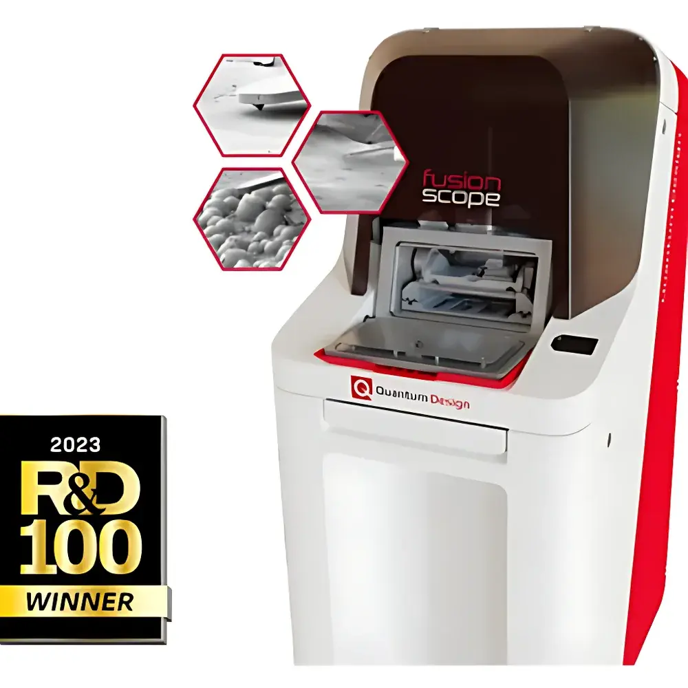
The Quantum Design FusionScope Hybrid SEM-AFM Microscope represents a paradigm shift in nanoscale characterization by integrating scanning electron microscopy (SEM) and atomic force microscopy (AFM) into a single, co-registered, in situ platform. Unlike conventional sequential or correlative workflows—where samples are physically transferred between instruments, risking contamination, positional drift, and environmental exposure—the FusionScope enables true real-time, coordinate-preserved multimodal imaging and measurement. Its core architecture is grounded in thermal field emission SEM for high-resolution secondary electron imaging (down to sub-5 nm resolution at 15 kV) and a self-sensing piezoresistive AFM system capable of sub-50 pm height noise and atomic-resolution topography under high vacuum (1–10 µTorr). The instrument leverages a shared sample stage, synchronized coordinate framework, and unified software interface to ensure that every AFM scan occurs at the exact location previously identified via SEM navigation—eliminating registration error and enabling quantitative correlation between surface morphology, mechanical properties, electrical conductivity, magnetic domains, and elemental composition (when equipped with optional EDS).
Key Features
- In situ co-registered SEM/AFM operation: Real-time SEM-guided AFM tip positioning with sub-micron accuracy; no sample transfer required.
- Self-sensing piezoresistive cantilevers: Eliminates optical alignment constraints; enables full signal access for C-AFM, MFM, EFM, and force spectroscopy while maximizing electron beam access to the probe–sample interaction zone.
- Profile imaging mode: Live cross-sectional view of the AFM cantilever relative to the sample surface—critical for targeting recessed, tilted, or suspended nanostructures (e.g., graphene membranes, bone lacunae, nanowire sidewalls).
- Automated multi-modal workflow: One-click switching between SEM imaging, AFM topography, and advanced AFM modes (FIRE, C-AFM, MFM, EFM) within a single experiment file.
- 80° simultaneous tilt capability: Coordinated rotation of both AFM probe and sample stage allows oblique-angle AFM measurements without repositioning—essential for sidewall metrology and anisotropic property mapping.
- FusionScope Task Panel: Guided, wizard-driven operation sequences reduce setup time and minimize user-dependent variability—particularly valuable in GLP/GMP-compliant environments.
Sample Compatibility & Compliance
The FusionScope accommodates diverse sample geometries and sensitivities: maximum diameter 20 mm (12 mm for correlated SEM/AFM mode), height up to 20 mm, and mass ≤500 g. Its high-vacuum chamber (<5 min pump-down) supports air-sensitive, beam-sensitive, and hydrated (via controlled humidity options) specimens—including biological tissues, 2D materials, semiconductor devices, and catalytic nanoparticles. The system complies with ISO/IEC 17025 requirements for measurement traceability and supports audit-ready data logging per FDA 21 CFR Part 11 when configured with electronic signature and user-access controls. All AFM force curves, SEM image metadata, and EDS spectra are timestamped, versioned, and stored in standardized HDF5-based experiment files—ensuring reproducibility across laboratories and regulatory submissions.
Software & Data Management
FusionScope Control Software provides dual-mode operation: Standard Mode for rapid acquisition and Advanced Mode for scripting, batch processing, and custom feedback loop configuration. It natively exports AFM data in Gwyddion-compatible formats and integrates third-party analysis libraries for quantitative roughness, modulus mapping (via Hertzian or Sneddon modeling), and phase-resolved EFM/MFM demodulation. All raw and processed data—including SEM micrographs, AFM height/error images, force-distance curves, and EDS maps—are embedded in a single .fusionexp container file. This ensures full experimental provenance: operator ID, instrument calibration logs, vacuum history, and detector gain settings are automatically archived. Offline analysis is supported on any Windows/Linux workstation without proprietary runtime dependencies.
Applications
- Semiconductor metrology: Sub-10 nm transistor gate inspection, contact resistance mapping on Cu/TiN stacks, and dielectric breakdown site localization via correlated C-AFM/SEM.
- 2D material characterization: Strain mapping in suspended graphene using real-time deformation monitoring during AFM indentation; domain identification in MoS₂ via concurrent MFM and topography.
- Nanomechanics: In situ nanoindentation on Si nanowires with simultaneous SEM visualization of plastic deformation; segmented force curves on pharmaceutical microparticles with heterogeneous surface chemistry.
- Magnetic materials science: Phase-resolved MFM of FeNi nanorods aligned on patterned substrates; grain boundary magnetism in duplex stainless steels at crystallographic interfaces.
- Life sciences: 3D collagen fiber reconstruction within bone lacunae; high-fidelity topography of diatom frustules without dehydration artifacts.
- Functional ceramics: Grain-boundary potential profiling in BaTiO₃ polycrystals using EFM at ±1.5 V bias—directly correlating local permittivity with microstructural features visible in SEM.
FAQ
How does FusionScope achieve true in situ SEM/AFM correlation?
It uses a common coordinate system anchored to the sample stage, with real-time SEM video feed overlaid onto the AFM control interface—enabling drag-and-drop tip placement with <1 µm uncertainty.
Can I perform electrical measurements without compromising SEM resolution?
Yes. Self-sensing cantilevers eliminate laser interference; the thermal field emission source maintains stable beam current during simultaneous C-AFM biasing and SE detection.
Is the system compatible with existing lab infrastructure?
It operates on standard 200–230 VAC, 50/60 Hz single-phase power (15 A); vibration isolation is recommended but not mandatory due to active damping in the AFM head.
What vacuum level is required for atomic-resolution AFM?
Atomic resolution on HOPG is routinely achieved at 3–5 µTorr—within the typical operating range of the integrated turbomolecular pumping system.
Does FusionScope support automated EDS mapping alongside AFM?
Yes. Optional Oxford Instruments X-MaxN EDS integration enables pixel-synchronized elemental maps registered to AFM topography—ideal for compositional–mechanical property correlations in battery cathodes or catalyst supports.


