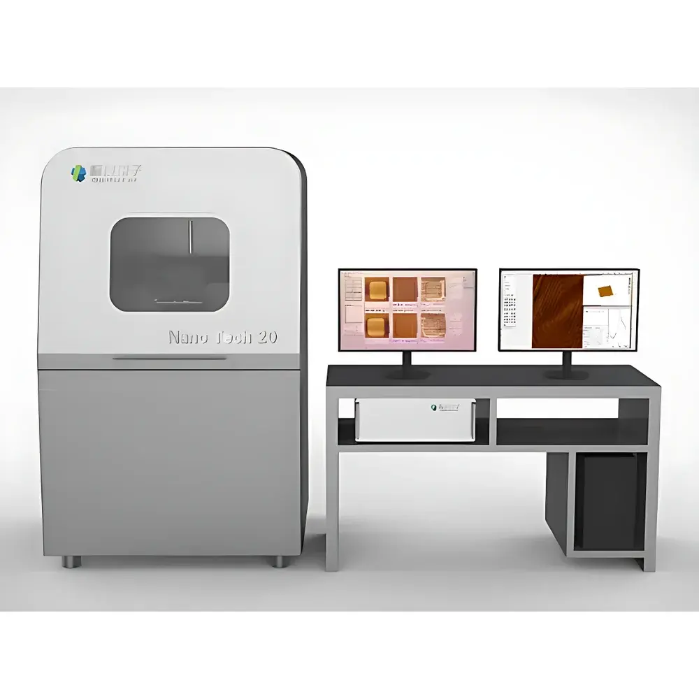
Quantum Scale Nano Tech 20 Atomic Force Microscope
| Brand | Quantum Scale |
|---|---|
| Origin | Jiangsu, China |
| Manufacturer Type | Authorized Distributor |
| Product Category | Domestic |
| Model | Nano Tech 20 AFM |
| Instrument Type | Industrial-Grade |
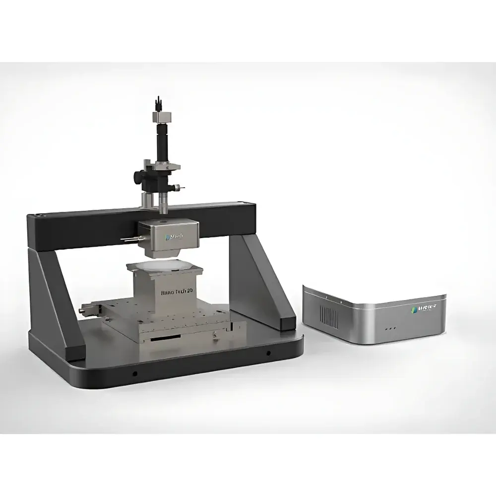
| SPM Architecture | Modular & Multi-Functional |
| Positioning Noise | XY: 0.2 nm, Z: 0.05 nm |
| Sample Size Compatibility | Up to 300 mm (12-inch) wafers, downward-compatible |
| XY Stage Travel | 200 mm × 200 mm (customizable) |
| Z Scan Range | 10 µm |
| Imaging Modes | Contact, Tapping, Force Spectroscopy, Phase Imaging |
| Optional Upgrades | EFM, MFM, KPFM, PFM, Lateral Force Imaging |
| Optical Microscope | 6.3 MP color CMOS, 7.5×–50× zoom, 34 mm working distance, 1.5 µm optical resolution at 50×, coaxial LED illumination, parfocal design |
| Scan Speed | 0.1–20 Hz |
| Feedback Bandwidth | 500 kHz (dual-channel lock-in), 18-bit amplitude/phase resolution |
| Data Acquisition | 16-bit, 100 kHz multi-channel sampling |
| Environmental Options | Vacuum mode (7.3 Pa base pressure), inert gas enclosure (N₂/Ar), H₂O/O₂ monitoring, temperature-controlled stage (−100 °C to +150 °C, ±0.3 °C stability), active air-sound shielding, pneumatic vibration isolation platform |
Overview
The Quantum Scale Nano Tech 20 Atomic Force Microscope (AFM) is an industrial-grade, modular scanning probe microscope engineered for high-resolution topographic and nanomechanical characterization in demanding R&D and quality control environments. Operating on the principle of piezoelectrically driven probe-sample interaction force detection, the system delivers sub-nanometer spatial resolution through direct physical feedback—enabling quantitative surface morphology, adhesion, elasticity, and electrical property mapping at the nanoscale. Its closed-loop XYZ positioning architecture ensures traceable dimensional metrology compliant with ISO/IEC 17025 reference frameworks. Designed for semiconductor wafer inspection, thin-film metrology, biomaterial surface analysis, and advanced material development, the Nano Tech 20 integrates a high-stability mechanical platform with real-time digital signal processing to maintain measurement integrity across variable environmental conditions—including controlled atmosphere, vacuum, and cryogenic or elevated temperature operation.
Key Features
- Sub-angstrom closed-loop noise performance: 0.2 nm lateral (XY) and 0.05 nm vertical (Z) positioning noise floor—validated under ISO 25178-6 metrological conditions.
- Modular SPM architecture supporting contact, tapping, phase, and force-curve imaging—upgradable to electrostatic force microscopy (EFM), magnetic force microscopy (MFM), Kelvin probe force microscopy (KPFM), and piezoresponse force microscopy (PFM).
- High-speed, multi-FPGA controller architecture: dual-channel lock-in amplifier with 500 kHz bandwidth, 18-bit phase/amplitude resolution, and configurable time constants from 0.5 µs to 100 ms.
- 200 mm × 200 mm motorized sample stage with programmable coarse approach and piezoelectric fine positioning—compatible with full 300 mm (12-inch) wafers and downward-compatible substrates.
- Integrated 6.3 MP color optical microscope with parfocal zoom optics (7.5×–50×), 1.5 µm optical resolution, and coaxial LED illumination—enabling precise probe navigation and region-of-interest targeting.
- Digital PID feedback controller with auto-engagement, real-time parameter optimization, and multi-channel synchronization for reproducible tip-sample engagement across heterogeneous surfaces.
Sample Compatibility & Compliance
The Nano Tech 20 accommodates rigid and soft samples up to 300 mm in diameter and 50 mm in height, including silicon wafers, glass substrates, polymer films, biological membranes, and composite coatings. Its environmental enclosure supports inert-gas purging (N₂, Ar), water/oxygen content monitoring (<1 ppm detection limit), and vacuum operation down to 7.3 Pa—meeting ASTM F1927 requirements for controlled-atmosphere surface analysis. Optional cryo- and thermo-stages operate from −100 °C to +150 °C with ±0.3 °C thermal stability, enabling in situ studies of phase transitions and thermomechanical behavior. The system’s mechanical design conforms to ISO 14644-1 Class 5 cleanroom compatibility when deployed with optional acoustic shielding and pneumatic isolation platforms.
Software & Data Management
The proprietary acquisition software provides simultaneous real-time visualization of CCD video feed, photodiode signal (PSD), and Z-piezo displacement—enabling intuitive probe alignment and dynamic mode tuning. All acquired data are stored in vendor-neutral HDF5 format with embedded metadata (timestamp, scan parameters, calibration history, environmental logs). The software supports GLP-compliant audit trails, user-access controls, electronic signatures per FDA 21 CFR Part 11, and automated report generation with NIST-traceable uncertainty estimation. Closed-loop single-point calibration routines ensure dimensional accuracy across the full 100 µm × 100 µm scan range, while batch-processing tools enable statistical roughness analysis (Sa, Sq, Sz) per ISO 25178-2 and power spectral density (PSD) computation per ISO 25178-3.
Applications
- Semiconductor process control: gate oxide thickness uniformity, CMP endpoint detection, lithography resist topography, and defect localization on 300 mm wafers.
- Advanced materials R&D: nanomechanical mapping of graphene monolayers, modulus gradients in gradient-index polymers, and domain structure analysis in ferroelectric thin films (via PFM).
- Life sciences: conformational dynamics of immobilized proteins, stiffness mapping of live cells under physiological buffer, and amyloid fibril growth kinetics.
- Energy materials: SEI layer morphology on battery electrodes, catalyst nanoparticle dispersion homogeneity, and perovskite film grain boundary analysis.
- Quality assurance: surface finish verification per ISO 4287, coating adhesion quantification via force-distance spectroscopy, and microscratch resistance evaluation.
FAQ
What vacuum level can the Nano Tech 20 achieve, and is it compatible with residual gas analyzers (RGAs)?
The system achieves a base pressure of 7.3 Pa in standard configuration; integration with external RGAs and turbo-molecular pumps is supported via flanged vacuum interface (CF35/KF40 options available).
Does the software support third-party scripting (e.g., Python or MATLAB) for custom automation?
Yes—the controller exposes a documented TCP/IP API and DLL-based SDK for programmatic instrument control, data streaming, and real-time feedback loop modification.
Is the system qualified for ISO/IEC 17025 accredited laboratories?
All critical subsystems—including Z-piezo linearity, XY stage repeatability, and optical microscope magnification—are supplied with factory calibration certificates traceable to NIST standards; on-site metrological validation services are available upon request.
Can the Nano Tech 20 perform correlative imaging with SEM or optical profilometry?
Yes—coordinate registration between AFM and complementary tools is enabled via fiducial marker alignment routines and shared stage coordinate referencing, supporting cross-platform data fusion workflows.
What maintenance intervals and service contracts are recommended for industrial deployment?
Preventive maintenance is scheduled every 12 months, including cantilever alignment verification, piezo hysteresis compensation, and environmental sensor recalibration; extended warranty and remote diagnostics packages are offered with SLA-backed response times.


